Nano-scale Control and
Detection of Electric Dipoles
in Organic Molecules
by
K.
Matsushige*, H. Yamada, H. Tanaka,
T. Horiuchi, and X. Q. Chen
Graduate School
of Engineering,
Kyoto University, Kyoto, 606-01 Japan
[email protected]
http://www.kuee.kyoto-u.ac.jp/index.html
This is a draft paper
for a talk at the
Fifth
Foresight Conference on Molecular Nanotechnology.
The final version has been submitted
for publication in the special Conference issue of Nanotechnology.
This page uses the HTML <sup> and
<sub> conventions for superscripts and subscripts. If
"103" looks the same as "103"
then your browser does not support superscripts. If "xi"
looks the same as "xi" then your browser does not
support subscripts. Failure to support superscripts or
subscripts can lead to confusion in the following text,
particularly in interpreting exponents.
Abstract
The nanoscopic ferroelectric domains could be formed in
P(VDF/TrFE) thin films by applying electric pulses with a
conductive atomic force microscope (AFM), and detected by using
piezoelectric response, revealing that the directions of electric
dipoles in organic molecules can be controlled in nano-scale. By
changing the polarity of the applied pulses, temporally stable
binary information could be "written" in this films.
Moreover, the possibilities of the molecular manipulation and the
creation of high-density molecular memory devices utilizing such
the electric interaction between the polar molecules and the
scanning probe microscopy (SPM) tips are discussed.
Introduction
In recent information technology, it is desired to store a
large capacity of digital data in a small size media. Although
there exist various types of memory devices such as CD (compact
disc) and MO (magneto-optical) disc and so on, the drastic
increase in their capacity can not be expected because of the
fundamental limitations as far as the laser lights with the
wavelength of several hundreds nm are used. Even the memory
devices utilized Si-based semiconductor technique, the similar
size limitations exist due to the lithography method, which use
lights, too. Therefore, one must seek and employ quite different
materials and novel write/read methods. Molecules are recognized
to contain themselves lots of information in the spatial
conformation and electrical characteristics. Among them, an
electric dipole may be one of the possible information units, if
the direction of the dipoles can be controlled in a nanometer
scale. Although ferroelectric organic thin films have gained much
attraction over the last several years because of its
technological applications such as piezo- and pyro-electric
devices, the ferroelectric nature has net been utilized to form
nanometer scale memories due to the lack of the manipulation
method for such the dipole orientation. While, SPM has been
demonstrated as a powerful tool not only for imaging surface
structures but for material modifications on nanometer scale
including atomic and molecular manipulations [1-2]. By using
inorganic ferroelectric thin films, it was reported that
nanometer-scale polarization domains can be created by a voltage
applied between a metal coated AFM tip and a conductive substrate
of the film [3-5] . One of the important parameters which
determine the size of the domain is the sample thickness because
the electric interaction area of the film is increased as the
thickness becomes large, and the ferroelectric properties in such
inorganic thin films often disappear due to some defects of the
structures / composition at the interface when the film thickness
is on the order of 10 nanometer or less. In contrast,
ferroelectric organic films are expected to keep the
ferroelectricity even in ultra thin films owing to its weak
interaction such as van der Waals force with the substrate.
Guthner et. al first demonstrated the formation and the
visualization of the micrometer-scale domains in ferroelectric
polymers films by SPM [6]. Also, the present authors successfully
observed the D-E hysteresis loop in the nano-scale area [7]. In
this study, we used Au-coated AFM conductive tips and a lock-in
amplifier measuring system to investigate local properties of
organic ferroelectric films and to demonstrate formation of local
polarization domains as small as 30 nm. The domains exhibited the
polarization reversal as well as the stable piezo response.
Finally, the possibility for the creation of the extremely-high
density molecular memory and the novel molecular nano-devices
using the ferroelectric molecules and SPM technique is discussed.
Experimental
The sample used in this experiments is copolymer
of vinylidene fluoride and trifluoroethylene with a molar ratio
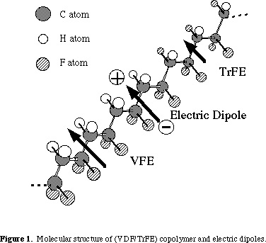
of 73/27. As shown in figure1, this polymer has electric dipoles
perpendicular to the molecular axis originated from the large
difference in the electron affinity of H and F atoms. The
copolymer samples were deposited on Pt substrate by a
spin-coating method. The Pt substrate was sputtered on silicon
dioxide. The sample was thermally annealed at 130 °C for 1
hour after the deposition to increase its crystallinity.
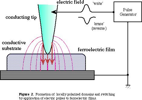
The polarization alignment and switching were
conducted by applying electric pulses to the film sample by using
an Au-coated conductive AFM tip, as shown in figure 2. The write
and erase procedure was done by changing the polarity of the
applied electric pulses. While, the ferroelectric domains was
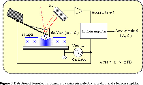
detected by utilizing piezo response as schematically shown in
figure 3. When we locate the tip on a polarization domain with
applying the oscillating weak electric field, piezoelectric
vibration is caused and the tip in contact with the film is
consequently vibrated. The vibration is detected using the
optical lever method and then the signal is demodulated by
lock-in 9/30/97amplifier so that both in-phase and quadrature
phase signals, i.e., both amplitude and phase information can be
obtained. In this setup the oscillation frequency used must be
located between the bandwidth of the feedback loop and the
resonant frequency of the cantilever. When the tip is scanned, it
follows the topography by feedback electronics but does not
follow the oscillation. Then both topographic image and
piezoelectric response can be simultaneously taken. From the
detected phase information, we can determine the polarity of the
domains, too. The Au coated tips and cantilevers had a spring
constant of 0.75 N/m and a resonant frequency of 88 kHz, and the
modulation signal applied to the tip had a frequency of 70 kHz
and a voltage of 0.5 Vrms.
Results and Discussion
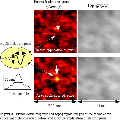
Figure 4 shows topographic and piezoelectric
response images of the ferroelectric copolymer film deposited on
Pt substrate, observed before and after application of the
electric pulse of -6 V with a duration of 1 second. As shown
clearly in these images, the bright spot with high piezoelectric
activity was created at the portion where the electric pulse was
imposed, although the corresponding topographic image taken
simultaneously does not show any change in its feature. Thus,
this fact suggests that the application of pulses can actually
form locally the ferroelectric domains as small as about 30 nm in
diameter. Here, it should be mentioned that the size of the
domains are governed mainly by the degree of the concentration of
electric field around the AFM tip, and so much smaller domains
can be expected to be formed if the AFM tips with more sharper
points are employed.
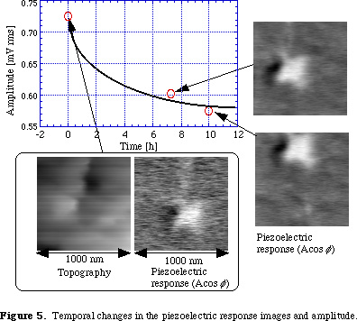
Next, the temporal stability of the polarization
domains formed by the application of electric pulses was
examined. Figure 5 show a series of such piezoelectric response
images observed at a fixed region. As the time passed after the
domain formation, the piezoelectric response became gradually
lower and attained at the level of about 80 % of the value at the
initial stage after 10 hours. The stability may depend on various
factors such as surrounding atmosphere, temperature, molecular
mobility of the ferroelectric polymers used, how frequently the
piezoelectric measurements which give mechanical and electrical
vibrations are done on the sample, and so on. Thus, although much
detailed investigations are necessary, it may be said that the
ferroelectric local domains can exist keeping their piezoelectric
activities for sufficiently long period time.
As revealed above, it became clear that the
ferroelectric domain with the sizes of several tens nm in
diameter can be formed locally at the desired points. In
addition, when the polarity of the applied electric pulses is
reversed, the piezoelectric responses are also reversed, forming
the ferroelectric domains with an opposite polarization
direction. By utilizing these evidences and imposing electric
pulses with positive and negative polarities during the scanning
of the AFM tip, one can write the binary information in series,
as depicted in figure 6.
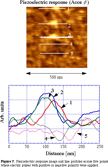
Figure 7 shows the piezoelectric response image
of the sample, for which the electric pulses were applied
repeatedly at approximately 100 nm separation. The lower figure
shows the line profiles across each formed domains, revealing the
polarity difference in the piezoelectric responses. These
evidences suggest that the novel molecular memory devices with nm
scale information units and so extremely high storage density can
be created based on the write/read method described here.
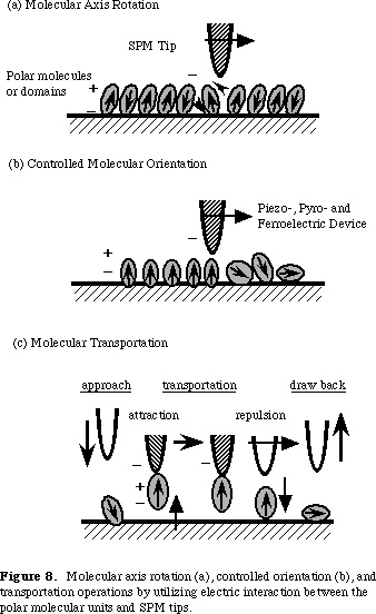
Finally, we discuss briefly the future
possibility on the nano-scale polar devices utilizing the
combination of the organic ferroelectric molecules and SPM
technique. In the organic ferroelectric materials as this case of
(VDF/TrFE) copolymer the electric dipoles exist with the
molecular structures and the ferroelectric domain can be formed
by controlling the molecular orientation. If we can develop the
conductive AFM tips with much sharper heads and employ the
molecular units which are composed of smaller crystalline units
of oligomers, and distributed separately within thin films or
individually on substrates, we will be able to change the
molecular direction and rotate the molecular units in nano-scale
level by using the electric force, and/or to control the
molecular orientation to create some nanoscopic piezo-, pyro-,
and ferroelectric devices, as schematically shown in figure 8 (a)
and (b). Furthermore, as shown in figure 8 (c), an attractive and
repulsive forces acting between the molecular dipole units and
AFM tips can be utilized to transport the each molecular units to
any desired positions, as seen in usual macroscopic world for
magnets. This kinds of nanoscopic operation using the electric
interaction will open new field of science, technology, novel
devices, and molecular electronics.
Conclusions
It was revealed that nanoscopic ferroelectric domains can be
formed in (VDF/TrFE) copolymer thin films by applying electric
pulses with conductive AFM tips, and detected by using
piezoelectric response. The formed ferroelectric domains were
found to be rather stable and the binary information can be
"written" by changing the polarity of the applied
electric pulses. Moreover, the possibilities of the molecular
manipulation and the creation of high-density molecular memory
devices utilizing the electric interaction between the polar
molecules and the SPM tips are discussed.
Acknowledgment
This work was partly supported from a Grant-in-Aid from the
Ministry of Education, Science, Sports and Culture, and KU-VBL
(Kyoto University-Venture Business Laboratory) project.
References
- 1) G. Binnig, C. F. Quate and Ch. Gerber, Phys. Rev.
Lett., 56 (1986) 930.
- 2) D. M. Eigler and E. K. Schweizer, Nature, 344 (1990)
524.
- 3) T. Hidaka, T. Maruyama, M. Saitoh, N. Mikoshiba, M.
Shims, T. Shiosaki, L. A. Wills, R. Hiskes, S. A.
Dicarolis, and J. Amano, Appl. Phys. Lett. , 68 (1996)
2358.
- 4) A. Gruverman, O. Auciello, J. Hatano, J. Vac. Sci. B
Technol., B14 (1996) 602.
- 5) A. Gruverman, O. Auciello, J. Hatano, A. Gruverman, J.
Hatano, Ferroelectrics, 184 (1996) 11.
- 6) P. Guthner and K. Dransfeld, Appl. Phys. Lett., 61
(1992) 1137.
- 7) H. Tanaka, H. Yamada, T. Horiuchi and K. Matsushige,
submitted to Appl. Phys. A.
Figure Captions
- Figure 1. Molecular structure of (VDF/TrFE) copolymer and
electric dipoles.
- Figure 2. Formation of locally polarized domains and
switching by application of electric pulses to
ferroelectric films.
- Figure 3. Detection of ferroelectric domains by using
piezoelectric vibration and a lock-in amplifier.
- Figure 4. Piezoelectric response and topographic images
of the ferroelectric copolymer film observed before and
after the application of electric pulse.
- Figure 5. Temporal changes in the piezoelectric response
images and amplitude.
- Figure 6. Binary information inputs by alternating the
polarity of the applied electric pulses.
- Figure 7. Piezoelectric response image and line profiles
across five points where electric pulses with positive or
negative polarity were applied.
- Figure 8. Molecular axis rotation (a), controlled
orientation(b), and transportation operations by
utilizing electric interaction between the polar
molecular units and SPM tips.
|