Organic Light Emitting Devices Fabricated from Semiconducting Nanospheres
Thomas Piok1, Stefan Gamerith1, Christoph Gadermaier1, Franz P. Wenzl1, Satish Patil2, Rivelino Montenegro3, Thomas Kietzke4, Ullrich Scherf2, Katharina Landfester3, Dieter Neher4 and Emil J.W. List*, 1
1Christian Doppler Laboratory Advanced Functional Materials, Institute of Solid State Physics, Graz University of Technology,
Petersgasse 16, A-8010 Graz, Austria
Christian Doppler Laboratory Advanced Functional Materials, Institute of Nanostructured Materials and Photonics,
Franz-Pichler-Strasse 30, A-8160 Weiz, Austria
2Department of Chemistry, BUGH Wuppertal,
Gauss-Str. 20 D-42097 Wuppertal, Germany
3Max Planck Institute of Colloids and Interfaces, Research Campus
Golm, D-14424Potsdam Germany
4Institute of Physics, University of Potsdam,
Am Neuen Palais 10, D-14469 Potsdam, Germany
This is an abstract
for a presentation given at the
11th
Foresight Conference on Molecular Nanotechnology
The trend towards nano-scale organic electronics raises a quest for novel materials and concepts which allow to control the deposition of the active material on the nano- to mesoscopic scale. Gaining control over the material at such a scale will enable the fabrication of novel as well as improved devices from organic semiconductors such as conjugated polymers in a cost-effective way. By adopting the so-called miniemulsion process one can combine the properties of semiconducting polymers with those of nanostructured matter, as has been shown recently.[2] Here a detailed and compressive study of organic semiconducting polymer nanospheres (SPNs) is presented. For a comprehensive picture the SPN's are directly compared with regular m-LPPP of the same patch.
The SPNs were characterized in detail in solution as well as thin films by means of transmission and photoluminescence spectroscopy and photo induced absorption experiments. Additional the films were characterized by optical, interferometric and surface probe measurements. Organic light emitting diodes (OLEDs) have been fabricated which have been deposited from aqueous dispersions by a spin cast process. Different batches of SPNs with different SPN diameters have been tested (69nm, 95nm, 126nm and 150 nm). The active layer of the devices consists of a single, homogeneous layer of the light emitting SPNs. All SPN-based OLEDs exhibit a light emission onset corresponding to the SPN energy gap (ca. 2.7 eV for m-LPPP, a semiconducting para-phenylene ladder polymer). Out of detailed surface studies via atomic force microscopy we propose that the low onset is attributed to field enhanced injection of charge carriers at the aluminum cathode due to the formation of stalactite-type nanostructures.
We show that the technique of miniemulsification also opens new perspective towards defined organic multilayer structures. Morphological characterization of such organic multilayers and their application in OLEDs will be discussed.
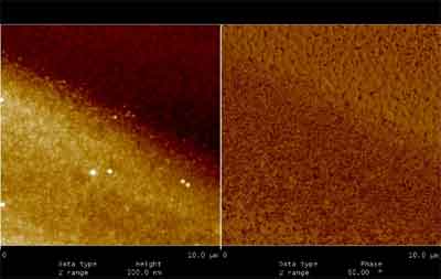 |
| Figure: AFM image (tapping mode) of a SPN monolayer spin-cast on top of a conjugated polymer (height image left, phase image right). |
References
[1] T. Piok et al., Adv. Mater. 2003, 15, 800.
[2] K. Landfester et al., Adv. Mater. 2002, 14, 651.
Abstract in Microsoft Word® format 461,126 bytes
*Corresponding Address:
Emil J.W. List
Christian Doppler Laboratory Advanced Functional Materials, Institute of Solid State Physics, Graz University of Technology,
Petersgasse 16, A-8010 Graz, Austria
Phone: ++43 316 873-8468 Fax: ++43 316 873-8478
Email: [email protected]
Web: http://www.if.tugraz.at/cdl/
|