Diamond Tip Arrays for Parallel Processing of Microelectromechanical Systems
Fumiya Watanabe*, a, Makoto Aritaa, Teruaki Motookaa, Ken Okanob, Takatoshi Yamadac
aDepartment of Materials Science and Engineering, Kyushu University, 6-10-1 Hakozaki, Fukuoka 812-81, Japan
bDepartment of Electronic & Photonics System Engineering, Kochi University of Technology, Tosa-Yamada, Kochi 782, Japan
cDepartment of Electrical Engineering, Tokai University, 1117 Kitakaname, Hiratsuka 259-12, Japan
This is an abstract
for a presentation given at the
Sixth
Foresight Conference on Molecular Nanotechnology.
There will be a link from here to the full article when it is
available on the web.
We have built a prototype system
capable of scanning probe microscope tip based parallel processing for
microelectromechanical fabrication. It utilizes uniform array of diamond
tips originally intended for field emission sources. Parallel patterns
are simultaneously fabricated on polymeric thin films spin coated on silicon
wafers. The processing line width of 100 nm is demonstrated. In addition,
a regularly spaced carbon islands have been deposited onto silicon surfaces
by simultaneous field evaporation. The diamond tip array method has potential
to greatly enhance nanoscale lithography and data storage derived from
proximal probe techniques whose shortcoming is the processing speed.
I. Introduction
Microelectromechanical systems have great
potentials to revolutionize all areas of science and technology by creating
sophisticated miniature devices. The basis of the microelectromechanical
systems fabrication is today's silicon processing technology mostly based
on optical lithography and wet or dry etching processes. The optical limitation
of such lithographic techniques will eventually force the semiconductor
industry to adapt new ways of processing ever smaller structures. Since
Eigler and coworkers have shown that a scanning microscope tip can be used
to manipulate single atoms, creation of nanoscale structures with scanning
probe microscopes (SPM) has been a popular subject of study. However, compared
to the optical lithography, the processing speed of SPM is too slow for
implementation in actual device construction. There have been some efforts
to construct parallel processing SPM devices with multi-tip cantilevers.
Most of these are delicate devices based on atomic force microscopes (AFMs).
We have proposed a apparatus with diamond tip arrays, called scanning
field emitter arrays (SFEAs), for parallel tip processing[1]. Simpler and
sturdier than the cantilever based AFMs, structures ranging from 100 nm
~ 300 µm have been fabricated on silicon surfaces by direct ablation
with the diamond scanning field emitter arrays. In addition, 1~25 µm
carbon islands have been deposited by field evaporation from the diamond
tips in air as shown in Fig. 1 below. We also present recent results on
patterning of polymer films spin coated on Si wafers with the diamond SFEA.
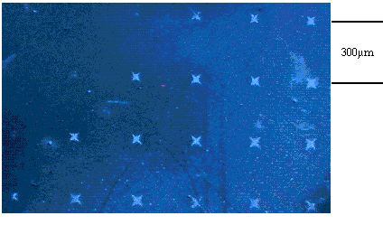
Fig. 1. Carbon islands simultaneously field evaporated from diamond tips (from ref. [1]).
II. Device Description
Diamond thin films are known to field emit at very low voltages in some
cases due to its negative electron affinity. And since diamond is very
stable both chemically and physically, it has become very popular material
to investigate for possible application in flat panel displays. Okano et
al. has developed an array of pyramidal shaped diamond tips utilizing pitted
silicon wafers as molds. The boron doped tips shown in Fig. 2 are approximately
50 µm in height and 70 µm at their bases, each separated by
the 7 µm wide channels. The approximate apex radius is 500 nm. The
size and the spacing are easily controlled by varying the silicon wafer
molds.
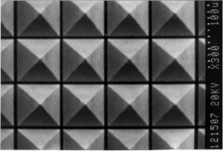
Fig. 2. SEM micrograph of diamond tip array with 7 µm spacings. The base of the tips is 70 µm long and their height is 35 µm for these tips.
Device used in this study is constructed from a hardness tester with
a diamond FEA mounted instead of a diamond indenter. The lateral (X and
Y) movements are by micrometers with better than 10 µm resolution,
and the vertical (Z) movements can be controlled down to 0.1 µm.
The array can be constructed with varying tip sizes and spacings. The ones
used in this study are approximately 2 mm x 2 mm, containing 40~600 tips
depending on the tip size and the spacing.
III. Experimental Results
The samples used in our trials are 20 mm x 20 mm chips cut out of a
boron doped Si(100) wafer. Si chip is chemically cleaned prior to the spin
coating by PVC solved in cyclohexanone (1 wt. %) at 2000 rpm for 50 sec.
The approximate thickness of the PVC film ranges from 100 to 200 nm.
The diamond tips were brought into contact with the PVC thin film coatings
and various patterns were drawn. Eleven pattern all ablated simultaneously
are recognizable in Fig. 3 below. The silicon wafer was later dipped in
a dilute HF solution. In Fig. 4, 150 nm wide line, left on the wafer after
the PVC film was removed, is given. In Fig. 3, some of the patterns are
missing indicating that there was some non-uniformness in the tip height.
The reason for this may be due to the deformation of substrate. In addition,
these patterns were drawn with the same tip array used in the carbon island
deposition and had some damages.
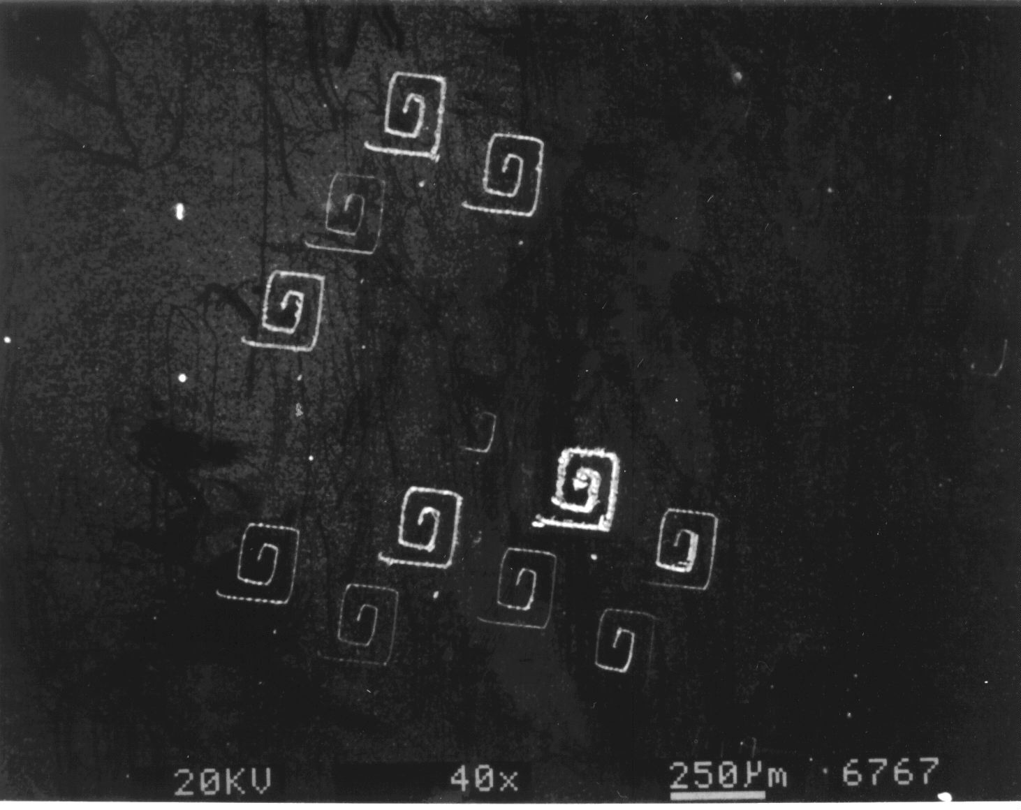
Fig. 3. Parallel patterns drawn on a PVC coated Si wafer before the etching in HF.
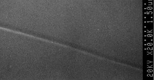
Fig. 4. SEM micrograph of a fine line feature created after HF dip of the diamond tip processed Si with a PVC coating.
IV. Conclusion
We have demonstrated a way for greatly enhancing the speed of SPM based
tip processing. Instead of relying on the fine control of tips, this device
utilizes the toughness of the diamond tips. To improve the performance,
we must rectify such factors as vibrational dumping, thermal stability,
and accuracy of scanning mechanism. The device should be equipped with
standoff columns which enable large size array to be placed on wafers directly.
Ultimately, these columns should contain piezoelectric material for scanning,
making the device a self sustained entity placed on a wafer. In addition
to semiconductor device processing such as fabrication of quantum dots,
SFEA may be a way of extending the abilities of other single tip techniques.
Since diamond has large band gap of ~5 eV, a properly formed tip can focus
light being illuminated from the back onto the apex of the tip with wavelength
down to the ultraviolet range. The diamond tip array may be suitable for
direct near field optical patterning of lithographic masks and thermomechanical
data storage.
Acknowledgement
This work was partially supported by a Grant-in-Aid from the Ministry of Education, Science, Sports, and Culture, Japan and by JSPS Research for the Future Program in the Area of Atomic-Scale Surface and Interface Dynamics under the project of Dynamic Behavior of Silicon Atoms, Lattice Defects and Impurities near Silicon Melt-Crystal Interface.
References
[1] F. Watanabe, M. Arita, T. Motooka, K. Okano, and T. Yamada, Jpn.
J. Appl. Phys. Part 2, Vol. 37, pp. L562-564, (1998).
*Corresponding Address:
Dr. Fumiya Watanabe
Department of Materials Science & Engineering, Kyushu University
6-10-1 Hakozaki, Higashai-ku, Fukuoka, 812-81 JAPAN
Phone: 81-92-642-3676; Fax: 81-92-632-0434
E-mail: [email protected]
|