Substrate Effects on Electronic Properties of Adatom Chains
Toshishige Yamada*
MRJ, NASA Ames Research Center, M/S T27A-1, Moffett Field, California 94035-1000
This is an abstract
for a presentation given at the
Sixth
Foresight Conference on Molecular Nanotechnology.
There will be a link from here to the full article when it is
available on the web.
When the device size is reduced down to 0.07 micrometers, the number of dopant atoms in the channel will no longer be macroscopic, typically less than a hundred. A spatial distribution of these dopant atoms will fluctuate statistically from device to device even in identically designed devices, and this places a serious limitation for integration. It is impractical to control dopant positions within atomic dimension. One fundamental solution to this problem is to create electronics with atomically precise, but preferably simple structures. Atomic chains, precise structures of adatoms created on an atomically regulated surface, are candidates for constituent components in future electronics. All the adatoms will be placed at designated positions on the substrate, and all the device structures will be precise, free from any deviations. It was predicted using the tight-binding calculation with universal parameters (Harrison 1980) that silicon chains were metallic and magnesium chains were semiconducting regardless of the lattice spacing (Yamada et al. 1996), and a possible doping method was also proposed (Yamada 1998).
In these treatments, the substrate was assumed to serve as a non-interacting template holding the adatoms without a formation of chemical bonding with substrate atoms. However, this scheme may not be easy to implement experimentally. Adatoms will have to be fixed with a van der Waals force on the substrate, but the force is generally weak and an extremely low-temperature environment has to be prepared to suppress their unwanted thermal displacement. It may be logical to seek a scheme to allow the adatoms to form chemical bonding with the substrate atoms and secure their positions. The substrate effects are studied in detail.
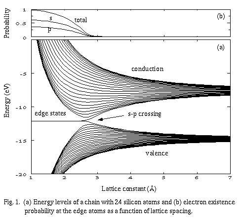
Once chemical bonds are formed, there is no guarantee that electrons are confined within a designated adatom structure. In the worst scenario, the independent adatom structures will interact strongly through an overlap of wave functions inside the substrate, resulting in large "crosstalk." This is not appropriate in device applications and must be avoided. It is shown (Shockley 1939) that if the substrate is made of crystals with a natural lattice spacing shorter than the s-p crossing point, dangling bonds of substrate atoms cannot penetrate into the bulk, and automatically localize at the surface. Examples for this type of substrate is a usual silicon crystal, a germanium crystal, a gallium arsenide crystal, and many metallic crystals like copper. Oppositely, if the lattice spacing is longer than the s-p crossing point, then there are no surface states of this kind, and all the modes penetrate deep into the substrate. Examples are alkali halide crystals, like sodium chloride. Apparently, we need to stick to the former s-p crossing substrate as long as the chemical bonding scheme is sought.
Figure 1(a) shows the energy levels of a one-dimensional chain created with 24 silicon atoms having an s-orbital and a p-orbital each (the remaining two p-orbitals are assumed to be used for other chemical bonding). As a gedanken experiment, the lattice spacing is changed from infinity to a finite value as the crystal is conceived of using the same tight-binding method. This is a mathematically simplified one-dimensional model to study the origin of surface states, and the surface states in this context correspond to edge states, where electrons strongly localize at the dangling bonds of the edge atoms. The figure shows that the edge states always appear in the middle of the band gap once after the s-p crossing has occurred. Figure 1(b) is the electron existence probability (s- and p-orbital amplitudes, respectively) at the edge atoms for these edge modes, and it is clearly seen that the electrons localize more strongly for shorter spacing. The edge states are quite robust, and their existence is not influenced by the detail of the lattice symmetry. It is also shown creating a similar plot that such edge states after the s-p crossing are eliminated when the dangling bonds are saturated with, e.g., hydrogen atoms.
This is because the participation of s- and p-orbitals are essential for the formation of edge states of this kind, while p-orbitals are irrelevant in a hydrogen atom. Therefore, we can use hydrogen atoms as if they were insulation materials. This is true regardless of the surface crystal-orientation as long as an s-p crossing crystal is used. The idea to use hydrogen atoms was proposed before (Watanabe at al. 1996), but it has not been discussed in the context of varying the lattice spacing.
The chemical bonding has two major effects on the chain electronic properties. First, only the remaining s- and p-orbitals not used for the chemical bonding can decide the chain band properties, rather than the full set of orbitals previously assumed. In fact, when two orbitals form a chemical bond, there appear bonding and antibonding states, separated by double the covalent energy, which is usually on the order of several electron volts. Two electrons, one of which is from the adatom and the other from the substrate atom, will occupy the bonding state and form a covalent bond, possessing much lower energy than the original. As a result, they cannot contribute to the chain properties, and one electron in the adatom is effectively eliminated per chemical bond. Second, because of a possible HOMO energy difference between an adatom and a substrate atom, semiconducting chains are unintentionally doped. These effects are studied with a self-consistent tight-binding method with universal parameters (Harrison and Klepeis 1988). With one adatom per unit cell, adatom chains are semiconducting (1) if adatoms are of group III and form one chemical bond per adatom, or (2) if adatoms are of group IV and form two chemical bonds. The previous result of realizing semiconducting chains by group II adatoms without chemical bonds is consistent with this picture. When the HOMO energy in an adatom is shallower than that in a substrate atom, the entire chain is positively polarized, unintentionally achieving p-type doping. When deeper, the chain is negatively charged, achieving n-type doping. A substrate significantly changes the electronic properties of the adatom chains and careful considerations are needed for electronics applications.
References
- Harrison, W.A. (1980) Electronic structure and the
properties
of solids (San Francisco, Freeman).
- Harrison, W.A.; and J. E. Klepeis (1988) Phys Rev B, 37,
pages 864-873. Dielectric screening in semiconductors.
- Shockley, W. (1939) Phys Rev, 56,
pages 317-323. On the surface states associated with a periodic
potential.
- Yamada, T. (1998) J Vac Sci Technol A, 16, pages 1403-1408.
Doping scheme of semiconducting atomic chains.
- Yamada, T.; Yamamoto, Y.; and Harrison, W.A. (1996) J Vac
Sci
Technol B, 14, pages 1243-1249. Energy band of manipulated atomic
structures on an insulator substrate.
- Watanabe, S.; Y. A. Ono; T. Hashizume; Y. Wada; J.
Yamauchi; and
M. Tsukada (1996) Phys Rev B, 52, pages 10768-10772. Electronic
structure
of an atomic wire on a hydrogen-terminated Si (111) surface: First
principles
study.
*Corresponding Address:
Toshishige Yamada
MRJ, NASA Ames Research Center
M/S T27A-1, Moffett Field, California 94035-1000
fax: 650-604-3957
E-mail: [email protected]
|