Nanostressing and Mechanochemistry
by
Kevin D. Ausman*, Henry W. Rohrs, MinFeng Yu, and Rodney
S. Ruoff
Department of Physics, Washington University, St. Louis, MO, 63130-4899
*Corresponding author: [email protected]
Web page: http://bucky5.wustl.edu
This is a draft paper for the
Sixth
Foresight Conference on Molecular Nanotechnology.
The final version has been submitted
for publication in the special Conference issue of Nanotechnology.
Abstract
Experimental evidence supporting the heightened chemical reactivity of
highly conformationally strained carbon sites in multi-walled carbon nanotubes
is reported. The strain is introduced by two methods, van der Waals
attractions to nonplanar surfaces and ultrasonic cavitation. Oxidative
acid attack was observed in both cases, in the former by etching of the
nanotubes' kinked sites, and in the latter by peptide coupling to polystyrene
spheres that are large enough to be visible by SEM imaging. A novel
single-axis straining stage for nanometer scale objects is also described.
Introduction
The remarkable mechanical and electrical properties of carbon nanotubes make them nearly ideal candidates for components in molecular machines and electronics. (Wong 1997; Treacy 1996; Cornwell 1998; Iijima 1996; Falvo 1997; Charlier 1998; Frank 1998; Kasumov 1998) Integration of these components into working devices, however, will require robust, well-defined connections, for which little is better than covalent functionalization. In addition, derivitization of carbon nanotubes has the potential to locally modify the intrinsic properties of the nanotubes. (Brenner submitted)
It has been observed that pristine carbon nanotubes are preferentially reactive at pentagonal defect sites, such as are commonly found at the tubes end caps. (Yao 1998; Satiskumar 1996; Ajayan 1993; Tsang 1993; Sloan 1998; Tsang 1994) This can be easily explained by the curvature effects introduced by these pentagons on the atomic orbital configuration of the carbon atoms. (Chen 1998a; Haddon 1996; Haddon 1993) Not only does this introduced curvature shift the hybridization of the atoms to a higher energy state, it also causes a decrease in the p-orbital overlap that causes conjugation. These effects are directly along the reaction coordinate for an addition reaction across an unstrained olefin, in which the carbon atom hybridization changes from sp2 to sp3. Thus the chemical reactivity of carbons at these strained sites is expected to be enhanced relative to unstrained, planar sp2 carbon.
For these reasons, the functionalization of carbon nanotubes is easiest at the end caps. (Wong 1998; Liu 1998; Satishkumar 1996) Though end cap derivitization will be necessary for the construction of nanotube-based devices, controlled, selective side wall derivitization would lead more easily to t-joint scaffolding and three-lead electronics devices. In addition, the end cap reactions explored to date, primarily oxidation, also lead to a small, uncontrolled degree of reaction along the side walls. (Lago 1995; Ebbesen 1996; Yu 1998; Chen 1998a) Though there has been a report of a designed carbon nanotube side-wall reaction, it was performed on nanotubes that had already been opened by oxidation, thus the relative reactivity between side wall sites and end cap sites was not explored. (Chen 1998a; Chen 1998b)
Thus, a more selective scheme for carbon nanotube derivitization that allows controlled reaction at specific sites along the otherwise undifferentiated side walls would be extremely useful. The introduction of local strain through conformational deformations, such as by kinking or twisting, will have similar effects on the atomic orbitals of carbon atoms as pentagonal defects, but to a degree that is controlled by the amount of local bending. This effect, observed fortuitously or by design in high resolution transmission electron micrographs (Iijima 1996; Ruoff 1995; Subramoney 1995; Kuzumaki 1998), will boost local reactivity at the kink sites significantly above that of the rest of the side walls. (Srivastava submitted) Unlike the strain introduced by pentagonal defects, however, the local strain is elastically introduced by reversible conformational distortions. (Wong 1997; Falvo 1997) Thus, after reaction, the nanotube could be straightened, leaving behind nanotubes selectively functionalized on the side wall.
In this paper we report the results of experiments aimed at exploring this proposed conformational-strain heightened reactivity of carbon nanotubes. In particular, we report results of reactions on nanotubes dispersed across a patterned surface that introduces conformational distortions in the tubes, and of reactions on nanotubes kinked in liquid suspension by ultrasonic waves.
Controlled mechanical manipulation and testing of nanostructures will be essential to the development and refinement of components for nanotechnology applications. In this paper we propose a design for a one-axis transmission electron microscope (TEM) compatible straining stage for nanometer scale objects. When applying tensile stress, this stage will allow determination of elasticity, yield-point, and tensile strength of nanoscale components or materials. Some of these properties have been measured for multi-walled carbon nanotubes by other methods involving thermal vibrations (Treacy 1996) or lateral bending (Wong 1997), but for geometric reasons the off-axis mechanical properties are likely to be different from the on-axis properties. When the proposed stressing stage is used to apply compressive stress, bending, kinking, and buckling may be observed. Furthermore, this stage may be used to pre-stress nanotubes for controlled kink-promoted chemistry experiments.
Experimental
Nanotubes on V-Ridged Substrate
A dilute suspension of multi-walled carbon nanotubes (donated by R. Smalley) was made in 2-butanol and then air-dried on a V-ridged silicon substrate (K-Tek TGG01). The peaks are 3.0 mm apart and 1.7 mm tall with a peak angle of 70°. The substrate was then exposed to nitric acid vapor at room temperature for 15 hours. Images of the tubes before and after the reaction were taken on a Hitachi S-4500 field emission gun scanning electron microscope (SEM).
Sonomechanochemistry
Multi-walled carbon nanotubes in surfactant/water solution were donated by S. Roth. These tubes had been purified and length-selected by size exclusion chromatography (SEC). (Duesberg 1998) SEC is the only carbon nanotube purification method in the literature that does not depend upon exposure to oxidative acids, which have the side effect of reacting somewhat with the nanotubes, leaving carboxylic functionality at the reaction sites. The nanotubes were redispersed in dimethylformamide (DMF) by repeated centrifugation, decanting, and sonication. Then one aliquot was reacted with concentrated nitric acid under reflux for 30 min. A second aliquot was reacted with concentrated nitric acid at room temperature in an ultrasonic bath for 30 min. Both samples were centrifuged, decanted, resuspended in DMF, and then reacted with thionyl chloride at 100 °C for 30 min. They were then centrifuged, decanted, washed with DMF, and then resuspended in a diluted solution of primary amine functionalized polystyrene microspheres (Bangs Laboratories, PA02N Lot 3427, mean diameter 100 nm). The resulting solution was then placed on silicon wafers, dried, and imaged by SEM.
Results and Discussions
Nanotubes on V-Ridged Substrate
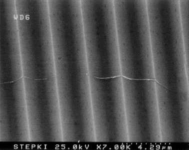 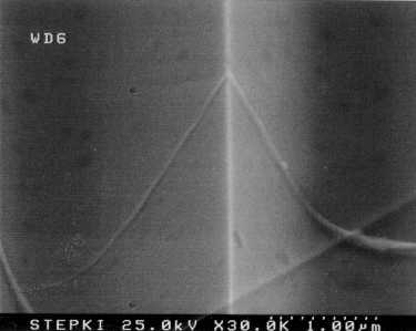
Fig. 1: SEM images of multi-walled nanotubes dispersed on V-ridge substrate.
Before reaction, the dispersed multi-walled nanotubes followed the surfaces
of the V-ridged substrate closely, as shown in Fig. 1. After extended
room-temperature reaction with nitric acid vapor, the kink sites at the
peaks of the ridges are observed to be selectively etched, as shown in
Fig. 2. The upper portions of the tubes are etched away, though the
bottom portion directly in contact with the surface may be intact.
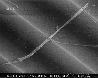 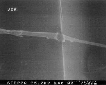
Fig. 2: SEM images of multi-walled nanotubes dispersed on V-ridge substrate
after extended exposure to nitric acid vapor.
Sonomechanochemistry
In these experiments, the oxidation by nitric acid should leave carboxylic
acid functionality at the sites of attack. The reaction with thionyl
chloride converts the carboxylic acid to an acid chloride, which then is
attacked by amines to form peptide linkages to the polystyrene microspheres.
These spheres were chosen to be an SEM visible tag to identify the sites
of oxidation.
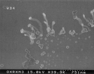 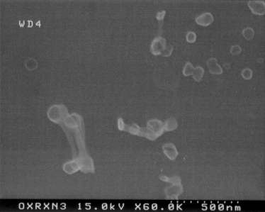
Fig. 3: Multi-walled nanotubes linked to polystyrene spheres by peptide
bonds.
As expected, the multi-walled nanotubes oxidized under reflux were thinned
and then end-cap coupled through peptide linkages to the amine-functionalized
polystyrene microspheres, as shown in Fig. 3. On the other hand,
the multi-walled nanotubes exposed only to room temperature nitric acid
under sonication exhibited less thinning and little amide coupling at the
end caps (Fig. 4). Instead, the polystyrene spheres attached to the
nanotubes at various points along their side walls. The simplest
interpretation of these data are that whereas refluxing nitric acid is
sufficient to attack nanotube end caps and etch away at the side walls
once attacked, room temperature nitric acid is too mild to do so.
However, the cavitation bubbles induced by sonication likely compress and
kink the nanotubes, locally creating regions of high curvature and thus
heightened reactivity.
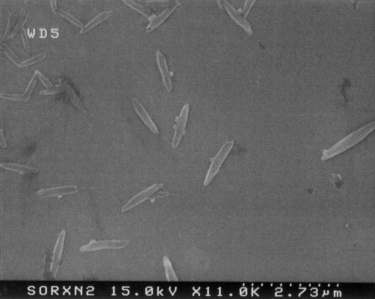 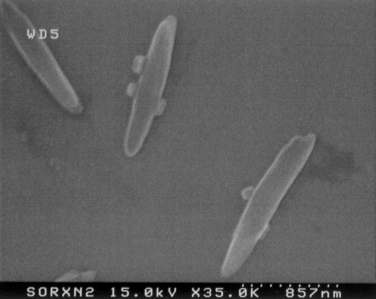
Fig. 4: Sonomechanochemically oxidized multi-walled nanotubes linked
to polystyrene spheres by peptide bonds.
These results strongly suggest that reversible conformational deformations
can heighten nanotube reactivity beyond that observed at pentagonal defects,
such as that which is observed at end caps. Individual nanotubes
kinked by scanning probe manipulation or by interactions with irregular
surfaces should allow controlled promotion of reactions at defined locations
along otherwise undifferentiated nanotube side walls. In bulk samples,
side wall reactivity can be heightened in a non-site-specific manner by
sonication.
Straining Stage for Nanometer Scale Objects
One would like to measure the mechanical properties of nanometer scale
objects directly. In the device shown in Fig. 5, we take a step in
that direction. This stage will be used to strain small objects while
observing their behavior in a TEM. Measurement of applied force will
be incorporated later. The stage will fit into probes manufactured
by Gatan.
The key component of the device derives from an etched silicon wafer.
The chip shown in Fig. 5 is 10mm x 10mm x 0.5mm. The pattern shown
consists of trenches and holes between 20 and 150 microns wide. These
will be etched through the wafer from the backside using deep reactive
ion etching. The size of the features makes the patterning amenable
to standard photolithography. In addition, the highly polished silicon
wafer will provide coplanar surfaces to which the test specimens will be
attached. Note that the overall height of the test stage in the vicinity
of the pole pieces of the TEM is only 0.5mm. Although this is not
shown in the drawing, the entire device will mount on a TEM probe or an
SEM holder.
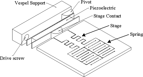
Fig. 5: Proposed straining stage for nanometer scale objects.
The silicon piece consists of a spring and a stage. The spring
allows the stage to move. When a force is applied at the contact,
the teeth of the stage will be brought closer together. The gap between
the teeth is decreased until it is small enough for the desired test.
For example, if one wants to probe the behavior of a 20nm section of a
carbon nanotube under a compressive or tensile stress, the gap would be
closed to this distance.
The most difficult part of any experiment conducted with this stage
will be setting the gap. We will use a fine screw (000-120) for this
and will monitor the gap using TEM and SEM. Such a screw moves about
210 mm per revolution and the lever shown will
reduce that by approximately one half. Since many of these will fit
on a wafer, we hope to make several stages with varying gaps. Thus,
we would bring the teeth together until we had a gap of 100nm or less then
set that stage aside and close the gap on another one. In this way
we hope to create stages to test objects between 10nm and 100nm.
Once the gap is set, the object of interest will be positioned across
it by dispersing the sample across the surface and manipulating the test
specimen using AFM or other means. Once in place and inside the TEM,
the specimen will be controllably strained by the expansion or contraction
of the PZT crystal. The plates that contact the PZT can be used to
hold a capacitive feedback device to monitor the movement of the crystal.
The test object will be continuously monitored with the TEM.
The TEM can be used to map out the behavior of a particular nanotube
vs. strain and the tube can be subject to the same forces outside the TEM.
Reagents for mechanochemistry can be placed directly on the stage in the
form of a drop or the stage could be dipped into a vial. After rinsing
and drying, the stage can be replaced in the TEM to observe the effects
of the chemical reaction.
Conclusions
Conformational strain heightened reactivity has been observed experimentally
on two samples of multi-walled carbon nanotubes. In one case, the
conformational strain was introduced by van der Waals attractions to a
non-planar surface, and the heightened reactivity was observed by oxidative
etching. In the other, the conformational strain was a result of
the high-pressure collapse of cavitation bubbles in an ultrasonic bath,
and the heightened reactivity was observed by coupling polystyrene spheres
through peptide linkages to sites of oxidative attack. A design for
a TEM compatible straining stage for nanometer scale objects was also described.
Acknowledgments
We would like to thank Drs. R. Smalley and S. Roth for the donation of
multi-walled nanotube samples. We also acknowledge Drs. B. Armbruster
and R. Zolkowski of Gatan Corp., Pleasanton, CA, Dr. L. Rathbun of the
Cornell Nanofabrication Facility, and Dr. T. Saif of the University of
Illinois, Urbana-Champaign for their help in the design of the nanostressing
stage. This work was partially supported by the NSF contract "New
Methods and Tools for Nanotechnology."
References:
-
Ajayan P M et al. 1993 Nature 362 522-525
-
Brenner D W, Schall J D, and Shenderova O A submitted
-
Charlier J C and Issi J P 1998 Applied Physics A- Materials Science
& Processing 67 79-87
-
Chen J et al. 1998a Journal of Materials Research 13
2423-2431
-
Chen J et al. 1998b Science 282 95-98
-
Cornwell C F and Wille L T 1998 Journal of Chemical Physics 109
763-767
-
Duesberg G S, Muster J, Krstic V, Burghard M, and Roth S 1998 Applied
Physics A: Materials Science and Processing 67 117-119
-
Ebbesen T W 1996 Journal of Physics and Chemistry of Solids 57
951-955
-
Falvo M R et al. 1997 Nature 389 582-584
-
Frank S, Poncharal P, Wang Z L, and de Heer W A 1998 Science 280
1744-1746
-
Haddon R C 1993 Science 261 1545-1550
-
Haddon R C and Raghavachari K 1996 Tetrahedron 52 5207-5220
-
Iijima S, Brabec C, Maiti A, and Bernholc J 1996 Journal of Chemical
Physics 104 2089-2092
-
Kasumov A Y et al. 1998 Europhysics Letters 43 89-94
-
Kuzumaki T et al. 1998 Philosophical Magazine A-Physics of Condensed
Matter Structure Defects and Mechanical Properties 77 1461-1469
-
Lago R M, Tsang S C, Lu K L, Chen Y K, and Green M L H 1995 Journal
of the Chemical Society-Chemical Communications 1355-1356
-
Liu J et al. 1998 Science 280 1253-1256
-
Ruoff R S et al. 1995 Fullerenes: Recent Advances in the Chemistry
and Physics of Fullerenes and Related Materials (eds. Ruoff R S and
Kadish K M) 557-562
-
Satishkumar B C, Govindaraj A, Mofokeng J, Subbanna G N and Rao C N R 1996
Journal
of Physics B-Atomic Molecular and Optical Physics 29 4925-4934
-
Sloan J, Hammer J, Zwiefka-Sibley M, and Green M L H 1998 Chemical Communications
347-348
-
Srivastava D, Brenner D W, Schall J D, Ausman K D, Yu M, Ruoff R S submitted
-
Subramoney S, Ruoff R S, Laduca R Awadalla S, and Parvin K 1995 Fullerenes:
Recent Advances in the Chemistry and Physics of Fullerenes and Related
Materials (eds. Ruoff R S and Kadish K M) 563-569
-
Treacy M M J, Ebbesen T W, and Gibson J M 1996 Nature 381
678-680
-
Tsang S C, Harris, P J F, and Green M L H 1993 Nature 362
520-522
-
Tsang S C, Chen Y K, Harris P J F, and Green M L H 1994 Nature 372
159-162
-
Wong E W, Sheehan P E, and Lieber C M 1997 Science 277 1971-1975
-
Wong S S, Joselevich E, Wooley A T, Cheung, C L, and Lieber C M 1998 Nature
394
52-55
-
Yao N et al. 1998 Journal of Materials Research 13
2432-2437
-
Yu R Q et al. 1998 Chemistry of Materials 10 718-722
|