Why are carbon nanotubes such excellent field emitters?
by
Jean-Marc Bonard, Jean-Paul Salvetat, Thomas Stöckli,
László Forró, André Châtelain
Département de Physique, Ecole Polytechnique Fédérale de Lausanne,
CH-1015 Lausanne, Switzerland
*Corresponding author: [email protected]
This is a draft paper for the
Sixth
Foresight Conference on Molecular Nanotechnology.
The final version has been submitted
for publication in the special Conference issue of Nanotechnology.
1. Introduction
Carbon, one of the most abundant elements in the Earth crust, is also one of the most fascinating, in particular because of the variety of materials it forms. It can appear as a transparent crystal, but also as black amorphous soot: seldom is such diversity found in nature. It shows several very stable crystal forms, with widely different properties. Diamond is composed of sp3 bonded carbon atoms arranged in tetrahedrons, and is insulating, transparent and one of the hardest materials. In contrast, graphite appears as layered sheets of sp2 bonded carbon atoms arranged in a hexagonal network, and is very soft, semi-metallic, shiny grey with one of the highest melting points.
Recent years have shown an intense renewal of interest for carbon science, provoked by the discovery in 1985 of buckminsterfullerene, or C60 , by Kroto, Curl, Smalley and co-workers [1] . C60 is a unique structure: it is actually a closed cage made of 60 carbon atoms arranged in pentagons and hexagons and showing an exceptional symmetry. It was soon realized that C60 was not the only stable cage structure, and that it was only necessary to have 12 pentagons close to the hexagonal network to create such a structure, as follows from Euler's theorem.
In the wake of the discovery of fullerenes, a number of new forms of carbon were identified in a very short period of time. In 1991, Iijima discovered closed tubular structures, consisting of nested cylindrical graphitic layers capped by fullerene-like ends with a hollow internal cavity
[2].
These structures have fascinating properties [3] . They can be metallic as well as semiconducting, depending on the tube geometry [4] . They show promising prospects for applications: they are mechanically extremely stiff and resistant to bending [5] , and their suitability as a tip for scanning probe microscopy has also been demonstrated [6] . They furthermore have proven to be very good electron field emitters [7] - [11] .
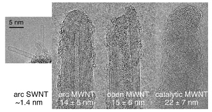
Carbon nanotubes appear in a large variety of forms, as shown in the transmission electron microscopy (TEM) images of nanotube tips of Fig. 1 . Singlewall nanotubes (SWNTs) have a mean diameter of ~1.4 nm, lengths that can reach several microns, and end in a spherical cap: they are thus one of the sharpest inorganic objects found in nature. Multiwall nanotubes (MWNTs) as produced by the arc-discharge (see section 2.1) have typically 5 to 10 times larger diameters, and show tips with a polyhedral shape. These tips can be removed by oxydation: the graphitic layers and the inner cavity are then exposed. Finally, nanotubes produced by catalytic reactions often show partially ordered layers containing extended structural defects. In the case of Fig. 1 , the graphitic planes are tilted with an angle of about 30° with respect to the tube axis, forming a piled-up "coffee-cup" structure.
Figure 1 - Transmission electron microscopy images of carbon nanotube tips, along with their mean diameter as determined from a statistical analysis.
We report here on the extensive characterization of carbon nanotube electron field emitters. We studied the emission behaviour of the four types of nanotubes displayed in Fig. 1 , as single emitters and in film form.
2. Emitter fabrication
2.1. Production of carbon nanotubes
The arc-discharge MWNTs were produced in a carbon arc apparatus using the method described by Ebbesen and Ajayan [12] , i.e., by arc discharge between two graphite electrodes (U = 16 V, I = 80 A) in a 350 mbar He atmosphere. These MWNTs were opened by heating in air at 550 °C for one hour and 620 °C for 12 min. [13] .
The SWNTs were produced by arc discharge under 500 mbar He static pressure using pure graphite electrodes 20 mm (cathode) and 5 mm (anode) in diameter. A 3 mm hole was drilled in the anode and filled with a graphite-Ni-Y mixture with weight proportion 2:1:1 [14] . The voltage and current used were approximatively 25 V and 100 A. The nanotubes were predominantely found in the webs, as opposed to the cathodic deposit.
The disordered nanotubes were produced by catalytic decomposition of acetylene on reduced cobalt oxide deposited on a silica substrate [15] . The nanotube powder was collected after dissolution of the silica substrate and catalyst in acid. In this case, the nanotubes show a high density of structural defects.
2.2. Single nanotube field emitter
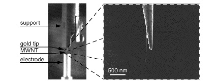
Single MWNT were mounted on a supporting gold wire (diameter 20 m) that was electrolytically etched to a ~250 nm radius tip. The tubes were held onto the tip by Van Der Waals forces. The tips were systematically characterized by SEM, as in Fig. 2 . Note that the tip needs not to have one single tube, since the emission from the second-best placed tubes will not contribute significantly to the emitted current.
Figure 2 - Single MWNT mounted on the tip of an etched gold wire (right image). For field emission, the gold wire is fixed on a support, and placed ~1 mm above the cylindrical counter-electrode (left image).
2.3. Nanotube film field emitter
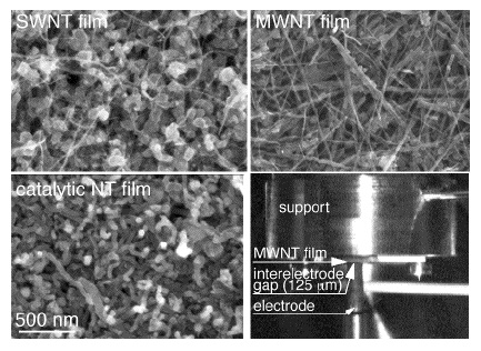
The nanotube films were realized by drawing a colloidal suspension of nanotubes through a 0.2 m pore silica filter, and by transferring this film on a teflon-coated metal surface [7] . The emission surfaces ranged from 0.1 to 25 mm2 , depending on the diameter of the filter, and are easily upscalable. Fig. 3 shows typical SEM micrographs of pristine films. The morphology of the films varied much with the type of the nanotubes. The arc-discharge MWNT films were made of randomly aligned, thin, straight and long tubes, while the catalytic ones were far thicker and curved. As for the SWNT films, they were composed of single tubes and ropes (assemblies of SWNT with a hexagonal lattice) lying on the surface along with catalyst particles coated with amorphous carbon. The average nanotube density amounted to ~109 cm-2 .
Figure 3 - SEM images of MWNT films taken at the same magnification. For field emission, the metal platlet which supports the film is mounted face-down on a support, and placed at ~125 m distance from the cylindrical counter-electrode (bottom right image).
2.4. Experimental set-up
For field emission, a 3 mm diameter cylindrical counterelectrode was placed at a distance from the tubes of 1 mm for the tips and 125 m for the films ( Fig. 2 and Fig. 3 , respectively). A Keithley 237 source-measure unit was used for sourcing the voltage (up to 1000 V) and measuring the current (with pA sensitivity), allowing the characterization of both single and cyclic (average) current-voltages (I-V) behaviour. The measurements were carried out at pressures between 10-7 and 10-9 mbar.
3. Emitter characteristics
3.1. Single nanotube field emitter
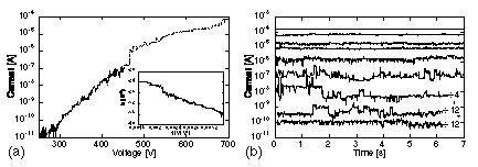
Fig. 4 (a) displays a typical I-V (current - voltage) characteristic for a single, opened MWNT emitter. At low currents, the I-V characteristics followed Fowler-Nordheim (F-N) behavior (i.e., metallic behavior, see Ref. [16] ). This can be seen in the inset of Fig. 4 (a) where ln(I2 /V) is plotted as a function of 1/V (F-N plot): F-N behavior is characterized by a constant slope in such a plot. Depending on the sample, the "metallic behavior" persisted up to 5 - 20 nA of emitted current.
At higher currents, the slope changed (by typically 10 - 30 %), increasing or decreasing depending on the sample, without discontinuities or instabilities in the I-V characteristics up to ~0.1 A. A very strong saturation with large instabilities was sometimes observed [10] .
When the voltage was further increased, an abrupt step appeared at 0.1 - 0.5 A, with the current increasing typically by one order of magnitude, as in Fig. 4 (a) where the measured current jumps from 0.17 A to 1.1 A between 464 and 466 V. After this step, most samples showed a monotonous increase of the current with the voltage.
Figure 4 - (a) single I-V characteristics for a single opened MWNT, with in inset the corresponding Fowler-Nordheim plot. Solid and dotted lines correspond to different ranges of the source-measure unit. (b) current stability versus time for the tube of Fig. 4 (a). The time scale for the three lowest traces has been divided by a factor 12 and 4, respectively.
It is worth notice that most single MWNT emitters, closed as well as opened, were capable of emitting over an incredibly large current range. The maximal current we succeeded to draw from one nanotube was ~0.2 mA, and MWNTs reached routinely and repeatedly 0.1 mA. This represents a tremendous current density for such a small object, and is actually quite close to the theoretical limit where the tube should be destructed by resistive heating [10] .
In Fig. 4 (b), we reported current stability measurements for the tube of Fig. 4 (a) over the whole explorated current range (~10 pA to 0.1 mA). We observed two different current regimes. At low currents, current switching between discrete current levels occurred. The frequency of switching between the steps increased with the current, with periods of stable emission covering more than 60 s at low currents (see Fig. 4 (b), bottom-most trace). This switching regime persisted up to 0.1 - 1 A, depending on the tip, which corresponded approximately with the position of the current step. Above the current step, stable emission with flicker noise was observed, with the signal-to-noise (S/N) ratio increasing with the current.
In
Fig. 5
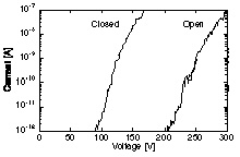
(a), we compare the I-V performances of closed and opened MWNT. We noted for all measured samples that opened tubes were far less efficient emitters than as-grown tubes. The voltages needed for a given emission current are typically a factor 2 higher for the opened tubes: the voltage increased from 190 to 400 V, and from 320 to 570 V, for 10 nA and 10 A emission, respectively. Quite surprinsingly, the emission characteristics of nanotubes are seriously degraded by opening their ends.
Figure 5 - Single I-V characteristics for a single closed and opened MWNT.
Finally, we estimate the field amplification factor from the I-V characteristics and corresponding F-N plots. In the frame of the Fowler-Nordheim model [16] , the slope of the F-N plot is equal to  , where B = 6.87·109 [V eV-3/2 m-1 ], f is the work function in [eV], d is the interelectrode distance in [m]. The field amplification factor b is defined as , where B = 6.87·109 [V eV-3/2 m-1 ], f is the work function in [eV], d is the interelectrode distance in [m]. The field amplification factor b is defined as  , where F is the field just above the surface of the tip, and V the applied voltage. We estimate the field amplification factor from the F-N slope in the low current regions, by taking f = 5 eV, as for graphite and C60. We are aware that this is valid only as an approximation, but it allows us nevertheless to compare the different emitters. For closed MWNT, the average field amplification factor was 40000 for 1 mm interelectrode distance, while it was about four times lower for the single opened MWNT tip (10800). , where F is the field just above the surface of the tip, and V the applied voltage. We estimate the field amplification factor from the F-N slope in the low current regions, by taking f = 5 eV, as for graphite and C60. We are aware that this is valid only as an approximation, but it allows us nevertheless to compare the different emitters. For closed MWNT, the average field amplification factor was 40000 for 1 mm interelectrode distance, while it was about four times lower for the single opened MWNT tip (10800).
3.2. Nanotube film field emitter
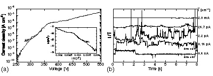
The behaviour of the films was readily comparable to the single emitters, as can be seen in Fig. 6 for a SWNT film. At low currents, Fowler-Nordheim behaviour was observed up to emitted current densities of 0.1 - 10 A cm-2 [ Fig. 6 (a)], with the F-N slope changing slightly at higher currents. At 10 - 100 A cm-2, a distinct diminution of the F-N slope (and therefore saturation) occurred on all samples. The current stability at constant applied voltage [ Fig. 6 (b)] depended again on the current (not on the applied voltage), and presented different current regimes. At low currents (< 10 - 25 A cm-2), current switching between discrete current levels was observed. The switching frequency increased with the current, with periods of stable emission as long as 240 s at low currents. At currents higher than 10 A cm-2 (which corresponded approximatively to the saturation point), the emission became gradually stable, without any detectable discrete levels with our time resolution of 10 ms. The S/N ratio increased with the current.
Figure 6 - (a) single I-V characteristics for a SWNT film with in inset the corresponding Fowler-Nordheim plot. Solid and dotted lines correspond to different ranges of the source-measure unit. (b) current stability versus time for the tube of Fig. 6 (a). The time scale for the two lowest traces has been divided by a factor 40 and 12, respectively.
We compare in the following the field emission performances of the four different types of nanotubes. Useful parameters for such a comparison are the turn-on voltage, Eto and the threshold voltage Ethr , i.e. , the electric field V/d needed to produce a current density of 10 A cm-2 and 10 mA cm-2 , respectively. These figures of merit correspond to typical values encountered in panel display applications. In Fig. 7 , we display averaged I-V characteristics around Eto (a) and Ethr (b). We found systematically that closed MWNT films emitted at lower voltages, followed by SWNTs, open MWNTs and finally catalytic MWNTs.
Figure 7 - Averaged I-V charateristics around (a) the turn-on field Eto and (b) the threshold field Ethr for different nanotube films.
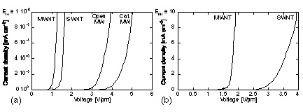
We listed in Table 1 the average values for Eto and Ethr obtained on five films or more for each type of nanotube (top part), as well as the values obtained on MWNT films by other groups along with our best devices (bottom part). Several conclusions can be drawn from this comparison. First, purification of closed MWNTs enhances the turn-on and threshold fields by a factor of two. Second, there are roughly two categories: closed MWNTs and SWNTs, with Eto ª 2.7 V/m and Ethr ª 5 V/m, and open and catalytic MWNTs, with Eto ª 5 V/m and Ethr ª 15 V/m. In particular, we note again that open MWNTs are by far less efficient emitters than closed MWNTs. Finally, our values compare readily to those obtained by other groups, although both used open MWNTs. However, their emitter fabrication method yielded tubes aligned with their axis perpendicular to the substrate, resulting in lower operating voltages.
Table 1 - Turn-on (Eto) and threshold (Ethr) voltages for various nanotube film field emitters. Top part: average values from this work. Bottom part: values obtained by other groups and our best devices.
|
Emitter
|
Eto
[V/m]
|
Ethr [V/m]
|
|
|
Arc MWNT
|
4.5
|
6
|
as grown
|
|
Arc MWNT
|
2.6
|
4.6
|
purified
|
|
Open MWNT
|
4.5
|
30
|
|
|
Catalytic MWNT
|
5.6
|
14
|
|
|
Arc SWNT
|
2.7
|
5.2
|
as grown
|
|
Open MWNT
|
1.5-7.5
|
1.9-9.5
|
Ref.
[9]
|
|
Open MWNT
|
0.9
|
3.7
|
Ref.
[11]
|
|
Closed MWNT
|
1.1
|
2.2
|
This work, best device
|
|
SWNT
|
1.5
|
3.9
|
This work, best device
|
We report in Table 2 the field amplification factor estimated from the constant F-N slope in the low current regime. In average, the field amplification factors were significantly higher for single- than for multiwall nanotubes films. This enhancement is most probably due to the smaller tip radius of SWNTs. The tip radius is also responsible for the low field amplification obtained with the catalytic tubes with respect to the closed MWNTs. However, the difference between closed and open MWNTs cannot only arise from geometrical considerations, since the variation of mean diameter and length between opened and closed MWNT is rather small (see Fig. 1 ). We speculate that most of this difference is due to changes in the work function that arise from the state of the tip (see also next section). In fact, the 1.5-fold decrease of b would correspond to a 1.3 fold increase in f .
Table 2 -
Average field amplication factors on nanotube films.
|
Emitter
|
Field amplification factor
|
|
SWNT films
|
3400
|
|
MWNT films
|
1600
|
|
opened MWNT films
|
1100
|
|
catalytic MWNT films
|
830
|
3.3. Comparison with other film emitters
In comparison to usual metallic emitters, the applied voltages needed for field emission were far lower for a comparable emitted current. For the single tips, currents of 1 A were typically obtained at 250 V. Interestingly, the only emitters which compete in terms of emission voltage with nanotubes films are the diamond-covered Si tips realized by Zhirnov et al. [17] . This indicates that maximal efficiency for film field emitters can be reached only (a) when the emitters are well aligned and placed with their long axis perpendicular to the film substrate, and (b) when the emitters are well separated from one another. These conditions are naturally realized in Spindt tips arrays, which are up-to-now the only industrially viable film field emitters. We thus infer that carbon nanotube films will have to be realized fulfilling the above-mentioned conditions to reach a maximal emitting efficiency. To our knowledge, the only method to grow aligned and well-separated nanotubes is by catalytic reactions over a patterned substrate, as currently investigated by several groups [18] [19] [20].
4. Field emission induced luminescence
During field emission, we furthermore observed luminescence on single- and multiwall nanotubes films as well as on single MWNT emitters [21] . The light emission occurred in the visible part of the spectrum, and could sometimes be seen with the naked eye. No light emission was detected without applied potential.
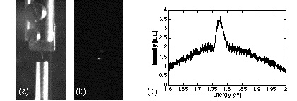
Figure 8 - (a) optical image of the experimental set-up for field emission and (b) corresponding field emission induced luminescence image for a single multiwall nanotube at 0.1 mA emitted current.; (c) Spectra of field emission induced luminescence for one MWNT at 10 A emitted current.
The emitted light intensity followed furthermore closely the variations in emitted current. Actually, the emitted intensity depends critically on the current, since the relative variations are 3-4 times higher for the luminescence as compared to the current.
To investigate further this phenomenon, we analysed the spectral repartition of the emitted light for single MWNTs. A typical spectrum is displayed in Fig. 8 (b). The spectra could be described with very good accuracy as a sum of two gaussian functions, with peak energies, widths, and relative intensities that varied with experimental conditions. The full width at half maxima (FWHM) in the case of Fig. 8 (b) were ~0.34 eV and ~22 meV for the broad and the narrow gaussian, respectively, with an integrated intensity ratio of typically 20. No significant changes in the shape of the spectra was observed when the current was varied apart from a small shift (<25 meV) of the broad gaussian. The position and width of the narrow gaussian remains nearly constant from one tube to the next. As for the broad gaussian contribution, we observed peak intensities and widths varying between 1.73 and 1.83 eV and between 0.3 and 1 eV, respectively. Finally, light was emitted at higher energies from SWNTs as compared with MWNTs.
There has been one report of observed luminescence on opened nanotubes [8] but it was attributed to an incandescence of carbon chains at the tip of the tube provoked by resistive heating. Our results however strongly suggest that the light emission is directly coupled to the field emission. The narrowness of the luminescence lines and the very small shifts with varying emitted current (< 5 meV) show that we are not in presence of blackbody radiation or of current-induced heating effects, but that photons are emitted following transitions between well-defined energy levels. This trongly suggests the presence of localized states at the tip.
We estimate that one emitted photon corresponds to at least 106 field emitted electrons. With localized states at the tip, the greatest part of the emitted current will arise from occupied states with a large local density of states located near the Fermi level. Other, more deeply located electronic levels may also contribute to the field emission. In this case, the emitted electron will be replaced either by an electron from the semi-metallic tube body with an energy comparable to the level energy, or by a tip electron from the main emitting state. Clearly, the second alternative may provoke the emission of a photon. Even if the tunneling probability for electrons from deep state is several orders of magnitude lower than for the main emitting state, it will be readily sufficient to cause the observed light intensities.
The luminescence intensity Ip as a function of the emitted current Ie follows a power law  with a = 1.4 0.2. This dependence can be reproduced by a two-level model [21] . The distribution of localized states at the nanotube tip is simplified to a two level system, with the main emitting level at energy E1 below or just above the Fermi energy, and a deep level at E2 < E1 . When an electron is emitted from the deep level, it is replaced either by an electron from the tube body, or by an electron from the main level which can provoke the emission of a photon. From the Fowler-Nordheim model, the transition probability D(E) can be evaluated for each level, and in the frame of our model, Ie D(E1), Ip D(E2). It appears that Ip varies as a power of Ie with an exponent that depends on the separation of the levels, and that amounts to 1.51-1.65 for the energies observed here (typically 1.8 eV), which corresponds well to the experimental observations. with a = 1.4 0.2. This dependence can be reproduced by a two-level model [21] . The distribution of localized states at the nanotube tip is simplified to a two level system, with the main emitting level at energy E1 below or just above the Fermi energy, and a deep level at E2 < E1 . When an electron is emitted from the deep level, it is replaced either by an electron from the tube body, or by an electron from the main level which can provoke the emission of a photon. From the Fowler-Nordheim model, the transition probability D(E) can be evaluated for each level, and in the frame of our model, Ie D(E1), Ip D(E2). It appears that Ip varies as a power of Ie with an exponent that depends on the separation of the levels, and that amounts to 1.51-1.65 for the energies observed here (typically 1.8 eV), which corresponds well to the experimental observations.
5. Field emission mechanism
We deduce from the above results that the field emission behavior of carbon nanotubes cannot be understood in terms of emission from a metallic tip. The luminescence and further measurements of the energy distribution of the emitted electrons [22] indicate that the electrons are emitted from narrow band states of ~0.3 eV half-width. In fact, theoretical calculations show that the local density of states at the tip presents sharp localized states that are correlated to the presence of pentagonal defects [23] . The observed luminescence strongly suggests that although the greatest part of the emitted current comes from occupied states with a large density of states near the Fermi level, other, deeper levels also contribute to the field emission. The position of the tip states with respect to the Fermi level influences directly the field emission properties of the tube. Indeed, only tubes with a band state close under or just over the Fermi level are good candidates for field emission.
6. Conclusions
We performed systematic studies of field emission on carbon nanotubes of different types. In comparison with other field emitters, operation voltages are ~5-10 times lower for comparable emitted currents. At low currents, the I-V characteristics follow the Fowler-Nordheim relation, but strong deviations from metallic behavior are systematically observed at high currents.
We observed significant differences in the emission characteristics between singlewall, closed and opened arc-discharge multiwall, and catalytically grown multiwall nanotubes. To obtain low operating voltages as well as long emitter lifetimes, the nanotubes should be multiwalled and have closed, well graphitized tips. The optimal emitters are thus closed arc-grown MWNTs. SWNTs degrade subtantially faster, as do MWNTs with disordered structures in addition to requiring high voltages for emission. Finally, the emission performances of MWNT nanotubes are seriously degraded by opening their ends
Our studies showed that the large field amplification factor, arising from the small radius of curvature of the nanotube tips, is partly responsible for the good emission characteristics. Additional studies [21] however showed that the density of states at the tip is non-metallic, appearing in the form of localized states with well-defined energy bands., which was confirmed by simulations. This fact influences greatly the emission behaviour. At and above room temperature, the body of the carbon nanotubes behave essentially as graphitic cylinders. This means that the carrier density at the Fermi level is very low, i.e., on the order of 5·1018 cm-3 , which is 3 orders of magnitude less than for a metal. Simulations show that the local density of states at the tip reaches values at least 30 times higher than in the cylindrical part of the tube. Since the field emission depends directly on this carrier density, the field emission current would be far lower without these localized states for a geometrically identical tip. The superiority of closed MWNTs over the other types is in this respect an additional indication, since the position and intensity of the localized states are strongly influenced by the crystalline structure. A disordered, or worse, a missing tip would consequently lead to inferior performances, as was observed for open and catalytic MWNTs.
Acknowledegements
The authors wish to thank Karine Méténier, Sylvie Bonnamy and François Béguin (CNRS-CRMD Orléans) for the growth of catalytic nanotubes; Revathi Bacsa (IGA-EPFL), Thierry Stora and Claus Duschl (LCPM-EPFL) for their help in the developement of the purification procedures; as well as Claude Blanc, Michel Fazan and André Guisolan (IPE-EPFL) for technical support. The electron microscopy was performed at the Centre Interdépartemental de Microscopie Electronique of EPFL. Financial support was provided by the Swiss National Science Foundation
References
-
H. Kroto, et al., Nature 318, 162 (1985).
-
S. Iijima, Nature 354 , 56 (1991).
-
M.S. Dresselhaus, G. Dresselhaus, and P.C. Eklund, Science of fullerenes and carbon nanotubes (Academic Press, New York, 1996).
-
J.W.G. Wildoer et al., Nature 391 , 59 (1998); T.W. Odom, J.-L. Huang, P. Kim, and C. M. Lieber, Nature 391 , 62 (1998).
-
M. R. Falvo et al., Nature 389 , 582 (1997). J.-P. Salvetat et al., submitted to Phys. Rev. Lett.
-
H. Dai et al., Nature 384 , 147 (1996).
-
W.A. de Heer, A. Châtelain, and D. Ugarte, Science 270, 1179 (1995).
-
A.G. Rinzler et al., Science 269, 1550 (1995).
-
P.G. Collins and A. Zettl, Appl. Phys. Lett. 69, 1969 (1996).
-
J.-M. Bonard et al., Ultramicroscopy 73, 7 (1998).
-
Q. H. Wang, et al., Appl. Phys. Lett. 70 , 3308 (1997).
-
T. W. Ebbesen and P. M. Ajayan, Nature 358 , 220 (1992).
-
D. Ugarte, W.A. de Heer, and A. Châtelain, Science 274, 1897 (1996)
-
W.K. Maser et al., Synthetic Metals 77, 243 (1996).
-
H. Alvergnat et al., Proc. Eur. Carbon Conf. (Carbon'96, Newcastle, UK), 715 (1996).
-
J. W. Gadzuk and E. W. Plummer, Reviews of Modern Physics 45, 487 (1973).
-
V.V. Zhirnov et al., 9th IVMC TechDig (1996).
-
W.Z. Li, S.S. Xie et al., Science 274, 1701 (1996).
-
G. Che et al., Chem. Mater. 10, 260 (1998).
-
M. Terrones et al., in Molecular Nanostructures, H. Kuzmany et al., Editors, World Scientific Publishing Company, Singapore (1998).
-
J.-M. Bonard et al., Phys. Rev. Lett. 81, 1441 (1998).
-
J.-P. Salvetat et al., AIP Conf. Proc. 442, 467 (1998).
-
D.T. Carroll, et al., Phys. Rev. Lett. 78, 2811 (1997).
|