Nanoscale Etching and Indentation of
Silicon (001) Surface with Carbon Nanotube Tips
by
Fedor N. Dzegilenko*, Deepak Srivastava, and Subhash Saini
IT Modeling and Simulation Group at NAS, NASA Ames Research Center, Mail Stop T27-A1
Moffett Field, CA 94035-1000
*Corresponding author e-mail: [email protected]
Web: http://science.nas.nasa.gov/~fedor/home.html
This is a draft paper for the
Sixth
Foresight Conference on Molecular Nanotechnology.
The final version has been submitted
for publication in the special Conference issue of Nanotechnology.
Abstract
The possibility of nanoscale etching and indentation of Si{001}(2 X 1) surface by (8,0) and (10,10) carbon nanotube tips is demonstrated, for the first time, by classical molecular dynamics simulations employing Tersoff's many-body potential for a mixed C/Si/Ge system. In the nanotube tip barely touching the surface scenario atomistic etching is observed, where as in the nanoindentation scenario nanotube tip penetrates the surface without much hindrance. The results are explained in terms of the relative strength of C-C, C-Si, and Si-Si bonds.
Introduction
Lithography plays a key role in semiconductor manufacturing. Currently surface patterning is achieved by means of optical lithographic techniques. However, with the industry moving towards the fabrication of semiconductor devices with the size features of 100 nm and less, [Road 1997] the ability of even deep ultraviolet light (193 nm) sources will be exhausted due to the absence of optically transparent materials at wavelengths significantly shorter than 193 nm. The technological community, thus, is actively searching for alternative approaches to materials fabrication at nanoscale. Among several alternatives to optical lithography are the utilization of high-resolution laser direct writing to structure silicon on the nanometer scale, [Mullenborn 1986] electron beam lithography, [Chang 1988] and proximal probe lithography. [de Lozanne 1993]
The proximal probe tips have been shown to be a powerful tool for the manipulation of individual atoms and molecules at the nanometer scale. [Gimzewski, Crommie 1993, Avouris, Huang 1997, Komeda 1997] A main difficulty faced in proximal probe lithographic techniques has been that the probe metallic tips often break following direct collision with the solid surface. Other alternatives to the metallic tips have been explored recently. Carbon nanotubes have been mounted on top of the silicon cantilever [Dai 1996] to be used as proximal probe tips. The carbon nanotubes are rolled-up sheet of graphene made of six folded benzene-type rings of carbon. The nanotubes are both of single and multi-wall (concentric cylindrical shells) nature and have unique elastomechanical properties. [Tersoff 1994, Yakobson 1996, Treacy 1996, Srivastava, Wang 1997] These are the strongest material known along the axial direction and yet are highly elastic and flexible along the radial direction.
Several groups have undertaken atomistic simulations of tip-surface interactions using models of usual metallic and/or diamond tips [Kallman 1993, Landman 1990,Harrison, Brenner 1996] interacting with diamond and/or silicon surfaces. In a recent study, [Dzegilenko 1998] we have simulated the possibility of selective etching of diamond surface by using a carbon nanotube tip chemically modified with a C2 species attached to the end cap of the tip. A single dimer of carbon atoms etched out of the surface by the tip, with the main result that the strongly bonded C2 chemical species on the tip is able to etch a weakly bonded C2 dimer from the surface. This raises the possibility that one can perhaps use a bare nanotube tip, made of strong C-C covalent bonds, for nano-lithography or atomistic etching on comparatively weaker bonded semiconductor surfaces such as silicon and/or germanium.
Using classical molecular dynamics (MD) simulations with Tersoff's potential for Si-C, Si-Si, and C-C interactions, [Tersoff 1989] in this paper we investigate the possibility of bare nanotube-etching and -indentation on silicon surfaces. The etching and indentation parameters are entirely determined by the mechanical properties of the tips and by the underlying tip-surface chemical reactions. Much of the complications involved in controlling the electronic behavior of the tip may be avoided. The possibility to pick up a single atom in field-free SPM regime has been recently experimentally demonstrated by Dujardin et al. [Dujardin] Single Ge atoms were extracted in a controlled manner from the Ge(111) surface by the ``traditional" SPM tip made of Ge atoms in a zero bias operation. Using MD simulations we show, for the first time, that similar atomic scale etching of Si surfaces is possible with carbon nanotube tips under zero bias operation conditions. The advantage of nanotube tip over the traditional metal or semiconductor tip would be that the nanotube tip can survive longer in experiments.
The model
The single-height-stepped Si{001}(2 X 1) surface has been chosen to model the surface of silicon. The slab representing the surface is composed of 15 full layers containing 128 atoms each and half-filled top layer representing the upper terrace of the stepped surface. The total number of atoms is 1984. The (8,0) carbon nanotube (composed of 222 carbon atoms) and larger diameter (10,10) carbon nanotube (composed of 470 carbon atoms) are used as tips as shown in Figure 1a and Figure 2a, respectively.
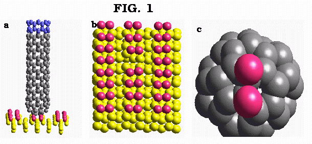
Figure 1a-c: Snapshots of reaction dynamics for the case when the (8,0) nanotube is initially directed towards upper-terrace site of silicon surface; a - nanotube is lowered onto the surface; b - final configuration of the silicon surface after the dimer abstraction; c - cap of the nanotube showing two Si atoms abstracted from the surface.
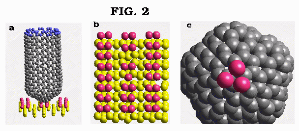
Figure 2a-c: Same as in Fig. 1a-c but for the (10,10) nanotube.
The caps of these two nanotube tips have different curvature and, as a result, the carbon atoms of the tip are expected to exhibit different chemical reactivity. Three different surface sites are considered. Those are the upper-terrace and lower terrace dimer on top sites and the dimer site at the step-edge. The dimer rows for lower and upper terrace are perpendicular to each other. The inclusion of step edge site allows to compare the reactive dynamics of the flat surface with the one near the step edge.
Tersoff's many-body empirical interatomic potential for multicomponent Si/C/Ge system has been used to describe the C-C and C-Si interactions. [Tersoff 1989] This is a reactive potential which allows for a description of bond formation and rupture. The bottom two layers of the silicon surface are held fixed. Next two layers are subjected to frictional and dissipative Langevin forces to drain out the excess kinetic energy and to hold constant the temperature of the system. The top two layers of the open end of carbon nanotubes are also constrained to vertically move the nanotube in a predetermined manner. Classical equations of motion are integrated using a third-order predictor-corrector method with variable time steps. Periodic boundary conditions are applied in the surface plane. Both interacting systems are initially equilibrated to 300K.
The nanotube vertical motion is achieved by displacing the constrained atoms at each (variable) time step in the desired manner. All the trajectories start with the distance between the specified surface dimers and the closest (to the surface) atom of the nanotube cap equal to approximately 6.5 Å which is well beyond the cutoff region of the C-Si interaction potential. Two regimes of nanotube tip operation are considered. In the first scenario the nanotubes move down and barely touch the surface mimicking the nanotube-surface chemical reaction induced by the vertical proximity of the nanotube and the surface. This is accomplished by downward displacement of the nanotube in 5000 variable time steps with 0.0013 Å displacement per step. In the absence of nanotube-surface interactions this approach velocity would place the nanotube directly on top of the surface dimers. The system is then equilibrated for 5000 additional steps and the nanotube is then pulled back. The nanotube displacement during the retraction phase is varied to slower velocities to ensure the convergence of the results. The per time-step retraction displacement of 5 times slower, than the value on the way down, is found to be the most computationally efficient without affecting the outcome of the simulations.
Results and discussion
For the (8,0) nanotube, the selective removal of the surface dimer occurs with minimum disturbance of the underlying silicon surface (Fig. 1b). The observed state configuration for the exit channel is linear. After a series of bond rearrangements, the atoms withdrawn from the surface are adsorbed on two neighbouring carbon atoms of the outer pentagon of the nanotube cap as shown in Fig. 1c. The results of simulations for a larger diameter (10,10) nanotube are shown in Fig. 2a-c. In the course of nanotube-surface chemical reaction, several lowest atoms of the nanotube cap form bonds with the surface. Finally, three silicon atoms are removed from the surface (Fig. 2b,c) via the distorted four member ring transition state at the exit channel. Similar to the previous case, the surface remains virtually undisturbed after the completion of mechano-chemical nanotube-surface reaction (Fig. 2c). Qualitatively similar results are observed for the lower terrace and step edge surface sites, though somewhat larger disturbance of the substrate is observed in the latter case.
In the second scenario, the nanotubes are pushed into the surface to make ``nano-holes". This ``digging" scenario allows the study of indentation phenomenon. Starting with the nanotube-surface distance of 8 Å,the nanotube is pushed down up to the nan otube indentation depth of 4 Å into the surface slab. The nanotube is then retracted similarly to the previous case.
The results of simulations when the (8,0) nanotube is allowed to penetrate inside the silicon slab are discussed next. Figure 3a shows the instance when the nanotube has indented and penetrated the silicon surface. The nanotube appears to completely preserve its original shape. The retraction of the nanotube causes adsorption of both the surface and bulk silicon atoms at the nanotube tip. At the end of the simulations, the internal structure of the silicon surface is strongly altered in the interaction region (Fig. 3b) though no apparent ``hole" is formed due to the ``healing" thermal motion of bulk surface atoms. Simulations with the substrate temperature reduced to 50K produced similar results. The main conclusion is that the indentation and penetration of silicon surface occurs easily and can be compared with the process of a knife cutting the butter. To compare the above with the contrasting behavior of the nanotube indentation on a harder diamond{001}(2 X 1) surface, the results are shown in Fig. 3c. In the nanotube indentation on the diamond surface, significant deformation of the nanotube is observed (Fig. 3c) and the diamond surface is not indented at all.
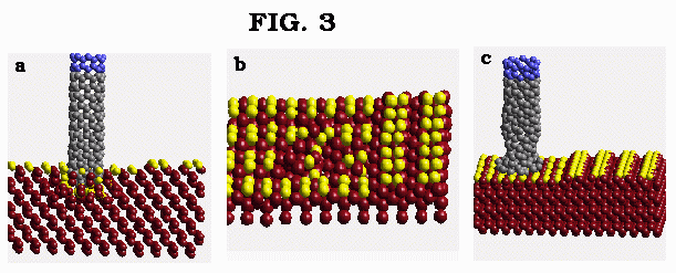
Figure 3a,b: Indentation of silicon surface by the (8,0) carbon nanotube; c) Compression of (8,0) carbon nanotube by the diamond surface.
In order to gain a better understanding of the details of the reactive dynamics, we have calculated vertical forces experienced by the tube and surface atoms during the nanotube-surface interaction period. The representative plots in the touching scenario (Figures 4a,b) show the vertical force on the nanotube atoms vs. the displacement of (8,0) nanotube towards the silicon surface. Zero of the x-axis corresponds to the initial vacuum nanotube-surface distance of 6.5 Å. The nanotube-surface distance varies in a complex manner and is not shown here. The surface layer position in the absence of nanotube-surface interaction is shown by arrows in the figure. Two curves shown in Fig. 4a correspond to the vertical force on the lowest two atoms of the nanotube tip, while those shown in Fig. 4b correspond to the forces on two silicon atoms of the upper-terrace surface dimer.
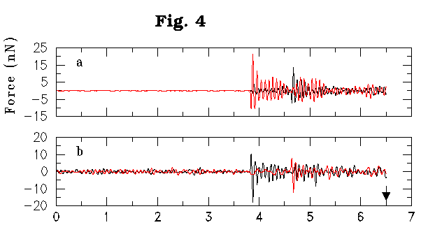
Figure 4a,b: Calculated vertical force (in Nano Newtons) for the two lowest atoms of (8,0) nanotube (a) and for the two surface silicon atoms of the upper-terrace site (b) versus the nanotube displacement towards the surface. Zero of the x-axis corresponds to the initial nanotube-surface distance of 6.5 Å. Arrow indicates the location of the silicon surface in the absense of nanotube-surface interaction.
No significant vertical forces are experienced by these four atoms until the nanotube displacement reaches 4 Å which will correspond to the nanotube-surface distance of about 2.5 Å in the absence of nanotube-surface interaction. At this moment, the sharp fluctuations of the vertical force are observed simultaneously for one of the nanotube atoms and for one of the surface silicon atoms indicating the formation of the first C-Si chemical bond. The formation of the second C-Si bond occurs later at the nanotube displacement of 4.7 Å indicating a sequential mechanism of the nanotube binding to the surface. Subsequent dynamics is dominated by a series of bond rearrangements and the atoms eventually lifted from the surface by the tip are shown in Fig 1c.
Figures 5a,b show the total vertical force experienced by (8,0) nanotube in the ``digging" scenario versus the nanotube displacement towards the silicon and diamond surfaces respectively. Zero of the x-axis corresponds to the initial vacuum nanotube-surface distance of 8.0 Å. Regular and identical patterns, corresponding to the excited phonon modes of the nanotube, are observed for both surfaces up to the nanotube displacement of 5.5 Å. This is because only upper-edge tip atoms of the nanotube a re uniformly displaced at each time step. At that moment significant fluctuations of the force start to appear as a result of interaction of the tip atoms with the surfaces. Both the variation and the magnitude of the force are significantly larger for the nanotube interacting with the diamond surface. This is consistent with the difference in the simulation outcomes for the silicon and diamond surfaces (indentation vs. compression, Fig. 3a-c).
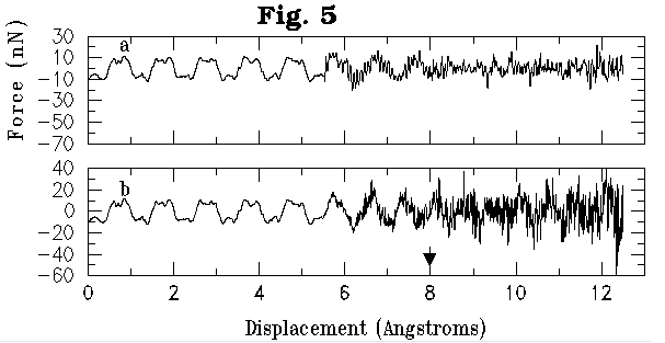
Figure 5a,b: Calculated total vertical force experienced by the (8,0) carbon nanotube during its indentation of silicon surface (a) and diamond surface (b) versus the nanotube displacement toward the surface. Zero of the x-axis corresponds to the initial nanotube-surface distance of 8 Å. Arrow indicates the location of the silicon and diamond surface in the absense of nanotube-surface interaction.
The effects of the long range van der Waals interactions on the above dynamics were also studied. Presently, there are no van der Waals interaction parameters tested with Tersoff's heteroatomic Si/Ge/C potential. To estimate the van der Waals interaction on the nanotube as it approaches a surface, we considered the nanotube interaction with the diamond surface including van der Waals C-C interaction parameters incorporated into the Tersoff-Brenner reactive potential. [Brenner 1996] The system is equilibrated first and then total energy minimization is performed at a variety of fixed nanotube-surface distances. The total van der Waals interaction potential from these calculations is slightly attractive all the way down to the tip-surface separation of approximately 1 Å where the net van der Waals repulsion kicks in. This is mainly because of the slope effect in the nanotube tip-surface interactions. Even for short tip-surface interaction distances, only bottom few atoms are in the van der Waals repulsive interaction regime. Majority of the tube atoms are in the attractive interaction regime and cancel the effect of repulsive interactions in the net interaction energies. Thus, the long range interactions do not introduce any barrier in the incoming channel and the van der Waals repulsion starts after the stronger chemical interaction is already in effect. For the nanotube-silicon surface, the effect of long-range interactions is expected to be even smaller than for the nanotube-diamond surface system because the interatomic distances within the silicon crystal are approximately 1.5 times larger than those of the diamond. Thus, we infer that the inclusion of long-range interactions will not significantly alter the reported results.
The observed results are qualitatively accounted for by the relative strength of interatomic bonds for the C-Si system. For the silicon surface, the interatomic Si-Si bonds within a silicon crystal are weaker than the corresponding Si-C bonds resulting in the removal of silicon atoms off the silicon surface (Fig. 1,2). At the same time, the C-C bonds which hold the nanotube together are stronger than both the Si-C and Si-Si bonds resulting in easy indentation of silicon surface by the nanotube, (Fig. 3) and the nanotube retains its original shape. The situation is quite the opposite for the diamond surface. The hierarchy of C-C bond strengths for the diamond-carbon nanotube system is the following: the strongest one is the C-C bond within a diamond crystal, the C-C diamond-nanotube bond is the next, and C-C bond inside the nanotube is the weakest one. This trend explains both the observed compression of the nanotube (Fig. 3) and the cleavage of the intrananotube bonds that was observed on the diamond surface (not shown here) in the ``touching" scenario.
Conclusions
In conclusion, we have demonstrated through classical MD simulations the possibility of selective etching and indentation of silicon surfaces by carbon nanotubes mounted on an scanning probe microscope cantilever. The proposed method is very robust and does not require applied voltage between the nanotube tips and the surface. We show that both the (8,0) and (10,10) nanotubes are able to extract silicon atoms off the silicon surface. The simulation results are timely in the sense that external voltage assisted nanotube-nanolithography [Avouris 1998,Dai 1998] and arrays of ``traditional" SPM tips in parallel [Quate] and tunnel-free [Dujardin] regimes have been recently demonstrated in experiments. The proposed method of etching of silicon surface combines the advantages of the above methods and provides additional input to the enabling technology for the next generation of SPM based lithographic techniques.
Acknowledgments
This work was supported by MRJ,Inc. under NASA contract NAS2-14303.
References
- [Road 1997] The National Technology Roadmap for Semiconductors SIA, San-Jose (1997).
- [Mullenborn 1986] Mullenborn M, in Frontiers in Nanoscale Science of Micron/Submicron Devices, Jauno A-K, Buzaneva E. V., editors (Kluwer Academic Publishers, Dordrecht), p 85. (1986).
- [Chang 1988] Chang T. H. P.,Kern D. P., Kratschmer E., Lee K. Y., Luhn H. E., McCord M.A., Rishton S. A., and Vladimirsky Y., IBM J. of Res. Develop. 32, 46 (1988).
- [de Lozanne 1993] de Lozanne A. L., Smith W. F., and Ehrichs E. E. Technology of Proximal Probe Lithography (Bellingham: SPIE Optical Engineering) p. 188 (1993).
- [Gimzewski] Gimzewski J. K., Jung T. A., Cuberes M. T., and Schlitter R. R., Surf. Sci. 386, 101 (1997); Tang H., Cuberes M. T., Joachim C., and Gimzewski J. K. ibid 115; Jung T. A., Schlittler R. R., Gimzewski J. K., Tang H., Joachim C., Science 271, 181 (1996).
- [Crommie 1993] Crommie M. F., Lutz C. P., and Eigler D. M., Science 262, 218 (1993).
- [Avouris] Avouris Ph., Lyo I-W, and Hasegawa Y. , J. Vac. Sci. Technol. A 11, 1725 (1993); Lyo I-W and Avouris Ph., Science 253, 173 (1991); Shen T-C, Wang C., Abeln G. C., Tucker J. R., Lyding J. W., Avouris Ph., Walkup R. E., Science 268, 1590 (1995).
- [Huang 1997] Huang D. H. and Aono M., Surf. Sci. 386, 166 (1997).
- [Komeda 1997] Komeda T., Hasunuma R., Mukaida H., Tokumoto H., Surf. Sci. 377-379, 149 (1997).
- [Dai 1996] Dai H., Hafner J. H., Rinzler A. G., Colbert D. T., and Smalley R. E., Nature 384, 147 (1996).
- [Tersoff 1994] Tersoff J. and Ruoff R. S., Phys. Rev. Lett. 73, 676 (1994).
- [Yakobson 1996] Yakobson B. I., Brabec C. J., and Bernholc J., Phys. Rev. Lett. 76, 2511 (1996)
- [Treacy 1996] Treacy M. M. J., Ebbesen T. W., Gibson J. M., Nature 381, 6781 (1996).
- [Srivastava] Srivastava D. and Barnard S., IEEE SuperComputing'97 (1997); Srivastava D. and Barnard S., in preparation.
- [Wang 1997] Wang E. W., Sheehan P. E., Lieber C. M., Science 277, 1971 (1997).
- [Kallman 1993] Kallman J. S., Hoover W. G., Hoover C. G., DeGroot A. J., Lee S. M., and Wooten F., Phys. Rev. B 47, 3318 (1993).
- [Landman 1990] Landman U., Luedtke W. D., Burnham N. A., and Colton R. J., Science 248, 454 (1990).
- [Harrison] Harrison J. A., White C. T., Colton R. J., and Brenner D. W., Surf. Sci. 271, 57 (1992); Sinnott S. B., Colton R. J., White C. T., and Brenner D. W., Surf. Sci. 316, L1055 (1994).
- [Brenner 1996] Brenner D. W., Sinnott S. B., Harrison J. A., Shenderova O. A., Nanotechnology 7, 161 (1996).
- [Dzegilenko 1998] Dzegilenko F. N., Srivastava D., Saini S., Nanotechnology 9, 325 (1998).
- [Tersoff 1989] Tersoff J., Phys. Rev B 39, 5566 (1989).
- [Dujardin] Dujardin G., Maine A., Robert O., Rose F., Joachim C., and Tang H., Phys. Rev. Lett. 80, 3085 (1998); Molinas-Mata P., Mayne A., and Dujardin G., Phys. Rev. Lett. 80, 3101 (1998).
- [Avouris 1998] Avouris Ph., Hestel T., Martel R., Schmidt T., Shea H., and Walkup R., ``Carbon Nanotubes: nanomechanics, manipulation, and functional electronic devices" preprint (1998).
- [Dai 1998] Dai H., Franklin N., and Han J., submitted to Science (1998).
- [Quate] Minne S. C., Manalis S. R., Atalar A., Quate C. F., J. Vac. Sci. Technol. B 14, 2456 (1996); Quate C. F., Surf. Sci. 386, 259 (1997) and references therein.
|