Thin Semiconductor Layers Prepared from Langmuir-Blodgett Precursor
by
Victor Erokhin1, Sergio Paddeu1, Cristina
Paternolli2, Alberto Leotti3 and Claudio
Nicolini1,2,3
*, 1Fondazione El.B.A., Corso Europa 30, Genova, 16132, Italy
2Institute of Biophysics, University of Genova, Corso Europa 30, Genova 16132, Italy
3Polo Nazionale Bioelettronica, Via Roma 28, Marciana (Li), 57030, Italy
*Corresponding author: [email protected]
This is a draft paper for the
Sixth
Foresight Conference on Molecular Nanotechnology.
The final version has been submitted
for publication in the special Conference issue of Nanotechnology.
Abstract
New ultrathin semiconductor materials were prepared by aggregation of
nanoparticles, formed in Langmuir-Blodgett precursors. Morphology of the layers
was studied by Brewster angle microscopy. Electrical conductivity of these
layers was studied in the plane of the layer. It was found, that contacts play
an important role in the conductivity of such ultrathin films of about 0.6 nm
thickness. These nanomaterials appear quite competitive for their high
resolution LB manifacturing with molecular beam epitaxy.
Introduction
Langmuir-Blodgett (LB) films of fatty acid salts was found to be
suitable materials for the formation of ultra small semiconductor particles in
them [1]. Films are placed into the hydrogen sulfide atmosfere and the
following reaction takes place:

where M is a bivalent metal, such as Cd, Pb, Hg etc., and n is ussualy equal to
16, 18 or 20. MS particles were found to be grown in a form of nanocrystals.
Other materials, not only fatty acid salts, can be also used for the formation
of semiconductor particles [2, 3].
Formation of ultrasmall semiconductor particles in LB film precursors allowed one to reveal some new phenomena, quantum in nature, such as blue shift of the absorbance spectra [1, 4] and single electron conductivity [5,6]. It was also shown the possibility to aggregate these particles into thin layers by selective removal of the organic molecules [4]. It was even shown with electron microscopy the possibility to form inorganic semiconductor superlattices by subsequent aggregation of nanoparticles formed in different LB precursor layers [7].
Aggregation of particles formed in LB film precursor allows to form ultra thin semiconductor layers with very high accuracy in the film thickness. It was found, that each bilayer of precursor results in about 0.6 nm of final inorganic film [4]. Only molecular beam epitaxy can provide such resolution. However, the proposed technique is more simple and does not demand specific expensive equipment. Therefore, the first step towards the utilization of such layers is to study their electrical properties. The present study is dedicated to a further investigation of such layers. The particles were formed by exposure of Langmuir-Blodgett films of arachidates with different metals (such as Cd, Cu, Zn) to the atmosphere of H2S. Morphology of the layers was studied by Brewster angle microscopy. Main attention was focused on the electrical properties of the layers.
Materials and Methods
Monolayers were formed by spreading the arachidic acid solution in chloroform at the surface of water subphase (water purified with Milli-Q system, resistivity of 18.2 W cm), containing 10-4 M of the desired ions. Langmuir films were formed and transferred onto substrates with LB trough (MDT, Russia) at 28 mN/m of surface pressure by vertical dipping. Glass substrates were used for the Brewster angle microscopy. Interdigitated Cr electrodes were used for the electrical characterization. The electrodes were deposited onto sapphire substrates. The digit length was 5 mm, the number of digits was 50 and the gap between them was 50 um. Time of the reaction with H2S was varied (from 20 min to 12 hour) according to the thickness of the film [4]. The particles were aggregated by the removal of fatty acid molecules with chloroform.
The morphology of the deposited layers was investigated by Brewster Angle Microscopy (BAM) [8] (Nanofilm Technologie GmbH, Gottigen, Germany, microscope type BAM 2). The Brewster microscopy allowed one to image 2D and 3D transformations which occurred before and after the reaction with H2S as well as to optimize the deposition procedure. The p-polarized beam light from a laser diode (l= 690 nm, 30 mW) was incident at the Brewster angle (56.5 °) to the air/glass interface and under such condition the reflected light was minimized. The presence of the film modified the Brewster angle so causing the reflection of the light beam, which was imaged by a CCD camera. The lateral resolution was of 2 µm and the images were 420 µm x 630 µm in size (512 x 768 pixels).
Electrical conductivity of these layers was measured by an electrometer (Keithley 6517, Cleveland, Ohio, USA) coupled with a Personal Computer by a GPIB-IEE-488.2 interface.
Results and Discussion
The results of the film morphology are presented for layers, prepared from Cu arachidate precursor (the results for other metals are similar). The BAM investigation of layers was performed after the deposition of the Langmuir-Blodgett films of fatty acid salts onto a glass solid support. Before the reaction with H2S a regular morphology was visible, i.e. a uniform covering of the surface was imaged (Figure 1 A). Microfractures and defects trough the film were also revealed and attributed mainly to dust particles incorporated during the deposition process. After the reaction with H2S, the morphology of layers was strongly changed due to the formation of nanoclusters resulting in a rearrangement of the organic matrix. As the result (Figure 1 B) initially uniform layer was transformed into a corrugated one. The presence of the interference rings in the image indicates significant differences in the thickness of the layer. Film of aggregated particles prepared by selecting removal of organic molecules with chloroform is composed of small aggregated crystals (Figure 1 C).
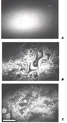
Figure 1: Brewster angle microscopy images. (A): 10 layers of Cu arachidate; (B): the same sample after the reaction with H2S; (C): the same sample after selective removal of arachidic acid molecules with cloroform.
Voltage-current characteristics of pure arachidates deposited onto interdigitated electrodes are presented in Figure 2. The characteristics present rather linear dependences. Small deviations from the linearity can be explained by the small values of the output current. Values of the specific resistance for all 3 types of arachidates are presented in Table 1.
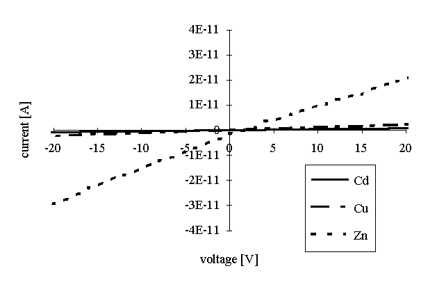
Figure 2: Voltage-current characteristics of the Cd arachidate, Cu arachidate and Zn arachidate LB films.
Table 1. Specific resistances of films prepared from different precursors at different stages of their formation measured on interdigitated electrodes.
|
arachidates
|
after
reaction
|
after
aggregation
|
Cd
|
1.55
x 1012 W cm
|
2.1
x 1010 W cm
|
1.3x
109 W cm
|
Cu
|
6.7
x1011 W cm
|
9.05x
109 W cm
|
5.2x
108 W cm
|
Zn
|
7.4
x 1010 W cm
|
3.2
x 1010 W cm
|
2.7x
105 W cm
|
After the reaction with H2S small particles were grown in the film. The presence of the particles varies the V/I characteristics of the layers (Figure 3). In fact, the characteristics became to be unlinear, making more difficult the calculation of the specific resistance. In order to obtain the parameter for comparison, specific resistances were calculated for the current values, corresponding to the voltage of 10 V. These data are also presented in Table 1. The specific resistance was reduced of about one order of magnitude for all three samples.
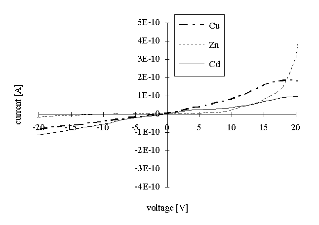
Figure 3: Voltage-current characteristics of the Cd arachidate, Cu arachidate and Zn arachidate LB films after the reaction with H2S.
V/I characteristics for the samples after aggregation (washing with chloroform) are presented in Figure 4 a (for CdS and CuS) and Figure 4 b (for ZnS). Specific resistance was also calculated for the current values corresponding to the 10 V of bias voltage (Table 1). In the case of CdS and CuS the specific resistances were reduced for one order of magnitude with respect to that before aggregation, while for the ZnS it was reduced for 5 orders of magnitude.
a 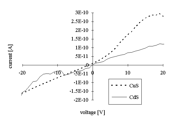
b 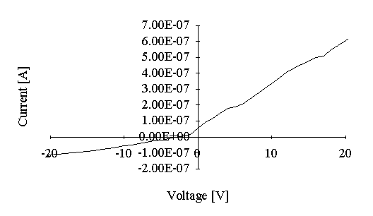
Figure 4: Voltage-current characteristics of the aggregated CdS, CuS (a) and ZnS (b) films.
Different steps of the film formation process are presented in Figure 5. Initially (Figure 5 a), the film is an insulating one. The conductivity is only due to the presence of defects. The difference in the conductivity for different samples can be explained by the different defect concentration.
Small semiconductor particles are formed in the film after the reaction (Figure 5 b). The conductivity, however, is still determined by the defects in the film, as these particles are not in a contact with each other and electrodes. The increase in the conductivity is due to the strong increase of defect number (see BAM image - significant corrugation of the layer).
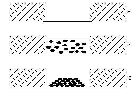
Figure 5: Schematic representation of the system under measurements: (A) initial LB precursor on the electrodes; (B) the film after the reaction with H2S; (C) aggregated film.
After the aggregation, the particles form rather homogenious layer, with average thickness of 0.6 nm per each bilayer of the precursor [4]. Particles are in a contact with each other. This fact results in a futher increase of the conductivity. Rather low level of the conductivity and difference for different samples can be due to the presence of potential barriers between individual granules. Moreover, it can appear regions of discontinuity near electrodes. In fact, the hight of the electrodes is much higher than the monolayer thickness and particle characteristic sizes. It will also result in the decrease conductivity. In order to check the last statement, the following experiment was performed.
Aggregated layer of CuS particles, formed from initial 30 bilayers of copper arachidate was prepared on the glass substrate. Electrodes were formed by In-Ga eutectic. V/I characteristics of such sample is shown in the Figure 6 (the characteristics, measured in the same configuration onto the bare glass is also presented for comparison; the current values in this case are much smaller than in a case of CuS layer and, therefore, practically coinside with X-axis). Slight difference of this characteristics from the linear one can be due to the not ohmic contact with eutectic or to the polycrystal nature of the layer. However, supposing this characteristics to be quasi-linear, it is possible to calculate the specific resistance, which was found to be about 200 Wxcm.
Comparison of this value with that in Table 1 allows to conclude that significan decrease in the conductivity is really due to the disontinuity regions near the contact of the layer with electrodes.
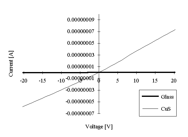
Figure 6: Voltage-current characteristics of the CuS aggregated films when contacts were formed by In-Ga eutectic (the characteristic for the bare glass is presented for comparison).
Conclusions
Layers of different aggregated semiconductors were fabricated. Their morphology at each stages of the formation process was studied by Brewster angle microscopy. Electrical characterization allowed to measure the conductivity of these layers. The values of the specific resistance were found to be dependent on the type of the material and on the way of the electrode preparation. Such layers can be useful for preparing semiconductor devices [9], when the thickness of the layer is a critical parameter.
References
- E.S. Smotkinm C. Lee, A.J. Bard, A. Campion, M.A. Fox, T.E. Mallouk,
S.E. Webber, and J.M. White, Chem. Phys. Lett., 153, 265-268
(1988).
- W. Huang, W.L. Lu, B.Y. Zhu, and G.X. Zhao, Mater. Lett., 33, 221-223
(1997).
- L.S. Li, L. Qu, L. Wang, R. Lu, X. Peng, Y. Zhao, and T.J. Li, Langmuir, 13,
6183-6187 (1997).
- P. Facci, V. Erokhin, A. Tronin, and C. Nicolini, J. Phys. Chem.,
98, 13323-13327 (1994).
- V. Erokhin, P. Facci, S. Carrara, and C. Nicolini, J. Phys. D: Appl.
Phys., 28, 2534-2538 (1995).
- P. Facci, V. Erokhin, S. Carrara, and C. Nicolini, Proc. Natl. Acad. Sci.
USA, 93, 10556-10559 (1996).
- V. Erokhin, P:Facci, L. Gobbi, S. Dante, F. Rustichelli and C. Nicolini,
Thin Solid Films, (1998), in press.
- D. Hönig and D. Möbius, J. Phys. Chem.,
95, 4590-4592 (1991).
- C. Nicolini, Thin Solid Films , 284-285, 1-5 (1996)
|