Wiring of metalized microtubules by electron beam-induced structuring
by
Wolfgang Fritzsche*, a, J. Michael Köhler,a Konrad J. Böhmb Eberhard Unger,b
Thomas Wagner,c Remo Kirsch,d Michael Mertig,d Wolfgang Pompe,d b
aMicrosystems Department, Institute of Physical High Technology, D-07702 Jena, PO Box 100 239, Germany
bInstitute of Molecular Biotechnology Jena
cFriedrich-Schiller-University Jena
dTechnical University Dresden
*Corresponding author: [email protected]
homepage
This is a draft paper for the
Sixth
Foresight Conference on Molecular Nanotechnology.
The final version has been submitted
for publication in the special Conference issue of Nanotechnology.
Abstract
Molecular electronics emerge as a possibility to continue the miniaturization of electronic circuits down to the lower nanometer scale. One significant challenge is the electrical connection of molecular devices by nanowires. We present here the realization of a new approach for wiring of nanostructures by linking metallized microtubule to prestructured microelectrodes. Microtubules (tube-like protein structures) were metallized and deposited on microstructured substrates. Electron beam-induced deposition (EBD) was used for structuring of connecting gold lines as nanoelectrodes, which wire a single microtubule to microelectrodes created by photolithography. First electrical measurements confirmed the suitability of the set-up for linking nanometer-scale structures to a measurement device. A metalized microtubule yielded a resistance below 50 Ohm over the length of one micron.
Introduction
The investigation of the electrical properties of small-scale structures is a fundamental issue of recent research in the field of nanometer-scale electronics. A prerequisite for electrical measurements is the wiring of the small structures, which represents enormous technical challenges due to the usually random distribution and the small feature size. A variety of techniques was developed to wire molecular structures dispersed on a planar substrate. First measurements of the resistance of a single carbon nanotube were reported for the chance occurrence of one nanotube spanning two lithographically patterned macroscopic electrodes (Whitesides and Weisbecker, 1994). Bundles of carbon nanotubes dispersed onto an oxidized Si wafer were located by scanning force microscopy and contacted by electron-beam lithography prior to electrical measurements (Bockrath et al., 1997). Four-probe measurement of individual carbon nanotubes based on focused-ion beam techniques were reported (Ebbesen et al., 1996). Another approach used a conductive scanning force microscope for measurements of carbon nanotubes in lithographically defined windows in a gold coating (Dai et al., 1996). Hybridization of complementary DNA was used for positioning DNA strands between microelectrodes prior to silver deposition along the biomolecule and electrical measurements (Braun et al., 1998).
We proposed another approach for connecting measuring devices to nanometer-scale materials, which is based on electron beam-induced deposition (Fritzsche et al., 1998). A gold coating of the substrate is masked by lines written with the scanning electron microscope (SEM). These lines connect the structure of interest (in our case a tube-like protein assemblate called microtubule) with prestructured electrodes. A dry-etching step removes the gold coating except the masked region below the lines. The presented paper extends this work by demonstrating electrical measurements. A biotemplated nanowire structure produced by electroless plating of metal onto the microtubule structure (Kirsch et al., 1997) was wired to microelectrodes prestructured by conventional photolithography. Electrical measurements demonstrate the successful realized wiring of the metallized biomolecules.
Materials and Methods
Microtubules
Microtubules (MTs) are intracellular proteinaceous elements with essential
functions in cell architecture and cellular transport, with dimensions in
the micrometer (length) and nanometer (width) range. They were purified
from porcine brain homogenates by temperature-dependent cycles of MT
disassembly/reassembly as described previously (Vater et al., 1995).
Microtubule metalization
The metalization of microtubules is described elsewhere (Kirsch et al.,
1997). Briefly, the protein structures were activated by adsorption of
Pt-catalyst particles using K2PtCl4 solution, followed by a metalization
using Ni acetate.
Substrates
Arrays of microelectrode pairs were prestructured from ~100 nm gold (primed
with a ~5 nm titanium layer) on a thermally oxidized silicon wafer
according to standard photolithographic techniques. The pairs had contact
pads of 400x200 µm (for convenient contacting by macroscopic electrodes)
connected to electrodes of 1 µm width, which were separated by a 12 µm gap.
Deposition onto the substrate
A droplet of diluted metallized microtubule solution was placed on the
prestructured substrates containing microelectrodes for approx. 1 min.
Then, excess water was removed with filter paper, and the specimen
air-dried. To monitor the position of the deposited microtubules, the
samples were examined in a low-voltage electron microscope Gemini DSM 982
(Zeiss, Oberkochen, Germany) at 1 kV.
EBD-line structures and gold contacts
For deposition of electron beam-induced deposited (EBD) lines the slow scan
axis of a SEM DSM 960 (Zeiss, Oberkochen, Germany) was disabled for usually
20 minutes. The repeated scanning results in the growth of an amorphous
carbonaceous film by polymerization of surface adsorbates (Broers et al.,
1976). This process is limited by surface diffusion. The deposition rate
depends on the total e--beam current density at the beam spot (and the rate
of emission of secondary and backscattered electrons), on the effective
adsorption rate onto the substrate, and on the probability for an electron
to cause EBD of a molecule (Folch et al., 1996).
For using the EBD-lines as masks a thin layer of gold (ca. 30 nm) was
sputtered onto the sample prior to the EBD structure. The gold was removed
by dry etching using Ar ions. Monitoring the electrical resistivity yielded
the degree of gold removal (by measuring the substrate) as well as the
masking efficiency of the EBD lines (by measuring control structures of EBD
lines).
Electrical measurements
Electrical measurements were conducted at room temperature in a two probe
way, using the auxiliary output ofa digital lock-in amplifier (SR850,
Stanford Research Systems) as a voltage source. The current was measured
with a low noise current amplifier (SR570, Stanford Research Systems).
Results and Discussion
Microtubules on microstructured substrates
Metallized microtubules (MTs) exhibit a typical bend appearance (Fig. 1) compared to native MTs which are usually straight along their whole length. This effect is probably due to growth stress of the spatially inhomogeneous growing nickel film and/or the diffusion of emerging hydrogen (Kirsch et al., 1997). The length of the metallized structures is in the lower micrometer range. The often observed branching of the structures can be explained by aggregation in the metalization solution.
The outer diameter of the metallized microtubules is between 50 nm and 100 nm (depending from the growth time) corresponding to a nickel film thickness of 15 to 40 nm. The metal film appears continuously. TEM investigations (Kirsch et al., 1997) revealed preferential nickel deposition on the microtubule surface from outside. Although nickel ions are expected to diffuse freely through the activated tubule wall, the lumen of the microtubules is not filled with nickel deposits. It is known that (in contrast to the lumen) the surface of microtubules exposes strongly negatively charged tubulin domains, which seem to bind the predominant part of the positively charged nickel ions. In addition, we assume that deposition in the lumen of the microtubules is prevented by the faster growing nickel film on the exterior surface of the tubules, "shielding" the lumen from nickel plating. Also the ends of the tubules are capped with nickel, hindering the deposition of Ni into the lumen.
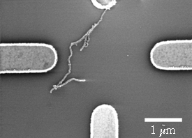
Fig. 1: Metallized MTs deposited on a substrate with
prestructured gold microelectrodes.
Localization of the molecules
The first step in wiring randomly distributed particles is the
localization. A typical microscopical methods for single molecule detection
in this size range is scanning force microscopy (cf. (Bockrath et al.,
1997)), but also the use of a focused-ion beam (FIB) system is reported
(Ebbesen et al., 1996). In the case of metalized MTs presented here a SEM
yields sufficient contrast for visualization (Fig. 1), compared to
insufficient contrast of native MTs in the SEM with the need of additional
SFM imaging in a previous study (Fritzsche et al., 1998). With the ability
of the SEM to visualize the MTs a combination of the visualization and the
structuring step is possible, thereby simplifying the whole technological
process.
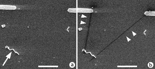
Fig. 2: Wiring of metallized MTs. a) A substrate with a MT
(arrow) near the electrode gap was gold coated (ca. 30 nm). b) EBD-lines
(arrow heads) were written to connect the MT with the microelectrodes.
EBD-line writing
The gold coating step, which creates a ca. 30 nm gold layer by sputter-coating, induces a slightly decrease in contrast (Fig. 2a). After positioning of the substrate the slow scan direction is enabled for about 20 minutes. The repeated line scan induces the polymerization of amorphous carbonaceous material along the path of the electron beam on the substrate (cf. (Broers et al., 1976; Folch et al., 1996)), which appears as a black line in the SEM contrast (Fig. 2b). A prerequisite for successful EBD-lines is the stability of the SEM, otherwise a broadening of the lines occur. Another parameters is the conductivity of the substrate, which enhances the growth. This phenomenon could be explained by charging effects suppressing the EBD effect.
Transfer of line structures into gold layer
The created EBD-lines have a low conductivity, which is insufficient for a direct use as electrical contact structures (Fritzsche et al., 1998). Therefore, the EBD-line is used as etch mask only for patterning of nanoelectrodes. Gold in form of a thin film was chosen as connecting material. Dry etch ing was used for the pattern transfer from the EBD-line into the layer. The control of this etching step is crucial for best results: overetching removes part of the sample molecule, uncompleted etching results in error currents along gold residues on the surface. Control structures (EBD-lines connecting two microelectrodes directly) were structured and the electrical resistance of these control structures and empty microelectrode gaps (i.e. without EBD-lines) were measured. Cycles of etching and measurement were repeated, until the empty gaps exhibit a high resistance and the control structure are still conductive.
Looping structure of metalized MTs
Molecules adsorbed on a liquid-solid interface are usually flattened after
air-drying. Metallized MTs exhibit freely suspended loops, which depart
from the substrate surface. This observation points to a stabilization
against the forces exerted by the receding meniscus during the drying
process. Because native MTs show no such loops (e.g., (Vater et al.,
1995)), the observed stabilization is probably due to the metal layer. The
looping structure presents a problem if the intersection of EBD-line and MT
is not directly attached to the substrate. In this case the gold line below
the EBD-structure (and therefore the electrical contact) would be
interrupted. So the MTs were carefully inspected in the SEM before EBD-line
writing to chose an appropriate region. On the other hand, this phenomenon
allows in principle conductive structures beyond the limit of conventional
planar technology.
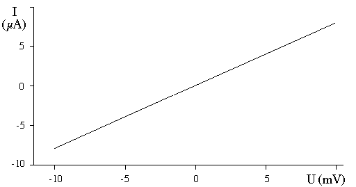
Fig. 3: Electrical characterization of a metallized MT at room
temperature.
Electrical characterization
The electrical characterization of a metallized MT-structure is given in Fig. 3. Because of the 2 probe set-up, the measured resistance includes the feed-lines and the contact resistance between the gold nanoelectrodes and the microtubules. The measured system yielded an Ohmic behavior. From control measurements over empty microelectrode gaps (which yields the resistance of the substrate) and short-cut microelectrodes (connected by an EBD-patterned gold nanoelectrode, which yields the resistance of the nanoelectrodes) we estimated the resistance over the microtubule being smaller than 50 Ohms. This value corresponds roughly with the expected resistance calculated from the geometrical data of a comparable hollow tube of pure nickel assuming an electrical resistivity for Ni of 7*10-8 Ohm m.
Limits of EBD-techniques
The EBD-phenomenon occurs not only in line scan mode, but with every contact of the electron beam with the surface. So also every imaging induces surface modification, although this effect is mostly insignificant. Only in the case of repeated positioning in SEM-imaging mode due to complex EBD-line geometries a darkening of the substrate was observed (Fig. 4). In this case, the EBD-layer will protect the underlying gold against the etching, resulting in a short-circuit. One could address this problem by creating empty microelectrode gaps with a comparable blackening by repeated scanning of the region, and use these gaps as controls in the etching / electrical measurement cycles.
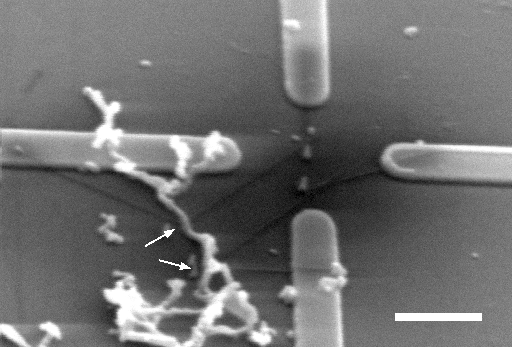
Fig. 4: MT-sample prepared for four-probe measurements. The two
measurement points on the microtubule structure are marked by arrows. The
upper point is wired to the left and the upper microelectrode, whereas the
lower point is connected to the right and the lower electrode. The wiring
EBD-lines are faintly visible as dark line structures. Bar = 2 µm.
Etching step
If the molecules are small compared to the thickness of the gold coating
(which was in our experiments 30 nm) the etching step could cause extensive
damage to the molecules. Compared to wet etching techniques, the dry etching has only low selectivity. We chose dry etching, because wet etching is diff
icult for the small feature size in the case of EBD-lines. A further
reduction of the gold coating thickness below 20 nm is possible, and would
result in a better control of the etching process against overetching.
In general, the etching is the limiting step of the proposed procedure. It
is time-limiting by the repeated etch/measurement cycles. In addition,
there is no absolute control of the etching process to achieve complete
gold removal without any damages of the molecular structure, so we
attempted to work with slightly damaged structures instead of a residue
gold layer.
EBD-approach
The combination of imaging and structuring tool is an advantage of the
presented technique. Localization, EBD-line writing, and a first
geometrical characterization of the created line structures can be obtained
by SEM in less than an hour. Because the EBD-growth relies on factors which
are not fully controlled in the used SEM (like the kind of gaseous residues
in the vacuum) an on-line monitoring of the EBD-line is essential for best
results. The methods needed (SEM and gold sputter coater) are available in
nearly any electron microscopical lab, only the dry-etching equipment is
less common. Therefore, the technique could be broad applicable without the
need to access sophisticated techniques like FIB (as in (Ebbesen et al.,
1996)) and electron beam lithography (as in (Bockrath et al., 1997; Dai et
al., 1996)).
Conclusions
We demonstrated in this paper the feasibility of a new approach for wiring of nanoscale structures. A EBD-based line writing was used for creating contact structures linking a nanowire (a biotemplated metal structure) to microelectrodes. A electrical characterization of the set-up demonstrated the feasability of the approach.
Further research will aim at four-probe measurements (Fig. 4) to separate the nanowire electrically from the surrounding electrodes. Another point is the use of thinner metal layers for metalization. An extension of the technique to other biomolecules (e.g., DNA) is planned.
References
- Bockrath, M., Cobden, D. H., McEuen, P. L., Chopra, N. G., Zettl, A.,
Thess, A. and Smalley, R. E. (1997). Science, 275, 1922-1925.
Single-Electron Transport in Ropes of Carbon Nanotubes
- Braun, E., Eichen, Y., Sivan, U. and Ben-Yoseph, G. (1998). Nature,
391, 775-778. DNA-templated assembly and electrode attachment of a
conducting silver wire
- Broers, A. N., Molzen, W. W., Cuomo, J. J. and Wittels, N. D. (1976).
Applied Physics Letters, 29, 596-598. Electron-beam fabrication of 80-Å
metal structures
- Dai, H., Wong, E. W. and Lieber, C. M. (1996). Science, 272, 523-526.
Probing Electrical Transport in Nanomaterials: Conductivity of Individual
Carbon Nanotubes
- Ebbesen, T. W., Lezec, H. J., Hiura, H., Bennett, J. W., Ghaemi, H. F.
and Thio, T. (1996). Nature, 382, 54-56. Electrical conductivity of
individual carbon nanotubes
- Folch, A., Servat, J., Esteve, J., Tejada, J. and Seco, M. (1996). J.
Vac. Sci. Tech. B, 14, 2609-2614. High-vacuum versus "environmental"
electron beam deposition
- Fritzsche, W., Böhm, K. J., Unger, E. and Köhler, J. M. (1998).
Nanotechnology, 9, 177-183. Making electrical contact to single molecules
- Kirsch, R., Mertig, M., Pompe, W., Wahl, R., Sadowski, G. and Unger, E.
(1997). Thin solid films, 305, 248-253. Three-dimensional metallization of
microtubules
- Vater, W., Fritzsche, W., Schaper, A., Böhm, K. J., Unger, E. and
Jovin, T. M. (1995). J. Cell Sci., 108, 1063-1069. Scanning force
microscopy of microtubules and polymorphic tubulin assemblies in air and in
liquid
- Whitesides, G. M. and Weisbecker, C. S. (1994). Mater. Res. Soc. Symp.
Proc., 349, 263.
|