3 Dimensional Manipulation of Carbon
Nanotubes under a Scanning Electron Microscope
by
MinFeng Yu1, Mark J. Dyer2, George D. Skidmore2, Henry W. Rohrs1,
XueKun Lu1, Kevin D. Ausman1, James R. Von Ehr2, Rodney S. Ruoff*, 1
1Department of Physics, Washington University in St. Louis, St. Louis, MO 63130-4899
2Zyvex L L C, 1321 North Plano Road, Suite 200, Richardson,
Texas 75081
*Corresponding author:
Physics Department, Washington University, CB1105, One Brookings Drive, St. Louis, MO 63130
Tel: 314-935-8746; Email: [email protected],
Web: http://bucky5.wustl.edu/
This is a draft paper for the
Sixth
Foresight Conference on Molecular Nanotechnology.
The final version has been submitted
for publication in the special Conference issue of Nanotechnology.
Abstract
Carbon nanotubes are manipulated in three dimensions inside a scanning electron microscope (SEM). A custom piezoelectric vacuum manipulator achieves positional resolutions comparable to scanning probe microscopes, with the ability to manipulate objects along one rotational and three linear degrees of freedom. This prototypical device can probe, select and handle nanometer-scale objects such as carbon nanotubes in order to explore and correlate their mechanical and electrical properties. Under real-time SEM inspection, carbon nanotubes are stressed while monitoring their conductivity, and nanotubes are attached to commercial atomic force microscope (AFM) tips such that the forces applied to the tubes can be measured from the cantilevers' deflections. The manipulator functions both as a research tool for investigating properties of carbon nanotubes and other nanoscale objects without surface restrictions, and as a rudimentary building device for larger nanotube assemblies. This capability to select and manipulate nanoscale components and to examine directly their suitability as construction materials during various phases of the construction process will play an important role in enabling the technology of assembling mechanical and electronic devices from prefabricated components.
Introduction
Recent theoretical and experimental investigations on carbon nanotubes(CNTs) indicate properties suitable for applications in the areas of nanoscale electronics, mechanics, and composites, among others. Depending on their size and helicity, single wall nanotubes(SWNTs) can be metallic or semiconducting, as has been calculated1,2 and measured experimentally.3,4 Multiwalled nanotubes(MWNTs) are found to be metallic. Quantum transport and single electron transport have also been observed.5,6 Devices such as a CNT quantum resistor and a room temperature, SWNT transistor have recently been reported 7,8 indicating that the application of CNTs to nanoscale electronics may soon play an inevitable and indespensible role in the development of nanotechnology. Because of the high in-plane modulus of graphite, CNTs should have high modulus, high tensile strength, and large reversible strain before tensile failure. Calculated values of Young's modulus for a SWNT range from 1 Tpa to 5.5 TPa, depending on how the cross-sectional area of the CNT is defined.9,10 Experimental measurements, by transmission electron microscope observation of the thermal vibrations of cantilevered multiwalled nanotubes 11and by lateral force microscope measurements on the bending of MWNTs give measured values of Young's modulus between 1 and 2 TPa.12 A calculated value for the strain at tensile failure of a single wall nanotube is ~ 40%,13 and deduction from an AFM experimental study of bending and buckling of MWNTs on silicon surfaces indicates a corresponding value of only 16%.14
The SEM manipulator is under development in part to investigate basic properties of single isolated CNTs with emphasis on characterizing their electrical and mechanical properties prior to incorporation into larger ordered networks or assemblies. Numerous electrical and mechanical measurements of CNTS have been conducted to a large extent on CNTs in contact with surfaces. However, the process of preparing and performing experiments on a single CNT using surface probes is typically tedious, and no studies to-date have reported liberation and handling of a CNT off the surface once it has been characterized. CNTs' properties might be greatly influenced by contact with a surface, for example, CNTs of certain diameter will flatten to some degree when in contact with a surface.15 It is also difficult to access all sides of a particular CNT if the tube is bound to a surface and only one side can be probed. It is thus advantageous to perform measurements on CNTs in free-space, and it is further desirable to have the capacity to manipulate a characterized CNT into position for device construction. A nanomanipulator inside an SEM permits viewing and placement of probe contacts at specified locations along a CNT, and with rotational freedom all aspects of the exposed CNT can be explored. Because operations can be viewed directly with high resolution under SEM, fewer ambiguities arise in interpreting the results from electrical and mechanical interrogations.
The extremely small size and variety of CNTs provide suitable challenges for the development of new tools and methods for their manipulation and for measurements of their properties. In order to construct devices with CNTs, along with other nanoscale components, such objects must presently be examined, characterized, and controllably manipulated into position within an integrated device. Ultimately, operations intermediate to the generation and integration of nanoscale components should proceed at high speed and be kept to a minimum if useful devices are to be mass-fabricated. We describe a method that can be applied both to fundamental research on CNTs and to the development of nanoscale construction protocols, and we present some preliminary results.
Instrumentation
A manipulation device inside SEM must perform a variety of functions for handling, characterizing, and building with CNTs and other small components. It should possess the ability and precision to probe a collection of CNTs, be it an ordered array or disordered bunch, then isolate the CNT and extract it from the collection. Once a CNT is isolated from the group, the manipulator must permit operations, both mechanical and electrical, necessary to characterize the strength and conductivity of the length of the individual CNT that is free from contact with a surface. Ideally, stretching, bending, twisting and compressing the tube at designated locations along the tube should be possible. The manipulator probes performing these operations should be metallic or metal-coated so that conductivity measurements can be carried out simultaneously. When suitable components are selected, the manipulator should permit transfer and construction operations, such as building three-dimensional CNT structures. It must further perform these operations without interfering mechanically with the microscope's components and without disturbing the electron microscope's imaging quality.
The SEM initially chosen to accommodate the manipulator is a JEOL T300 microscope with a secondary electron detector, which has a roomy sample chamber. The resolution of the microscope is specified as 6 nm at 30 kV. In practice, manipulations are performed under video imaging or slow-scan mode; the real-time video resolution is a factor of two or three lower, but high resolution photographic recording yields results close to the manufacturer's specifications of 6 nm.
The design of the manipulator is depicted in Figure 1. For clarity, the electrical connections and grounded shields are removed and only the major components are shown. This version of the SEM manipulator is constructed with commercially available stages and actuators. The manipulator was designed with wide translation range, reasonable precision, small size, low-cost, and rapid assembly in mind. To avoid interference with the SEM electron optics, the x-y and z-theta motions are grouped into two low-profile, opposing stage sub-modules anchored symmetrically on the SEM platform around the axis of the electron beam column. Coarse 3-axis linear motions up to 6 mm and single-axis 360 degree rotational probe motion are provided by vacuum-prepared stainless steel stages (OptoSigma) driven by similarly prepped Picomotor piezo actuators (New Focus). An integral X-Y stage guides motion parallel to the plane of the SEM stage, and a separate Z-axis stage is used for motion along the SEM beam axis. Rotational motion normal to the beam is accomplished using a Picomotor rotating actuator mounted atop the Z-stage. This actuator is attached mechanically to a chemically-etched tungsten tip with an electrically-insulating Delrin coupling. The length of the tip passes through a ceramic bushing bonded to the tip end of a piezo tube, which is mounted coaxial to the rotating actuator. The 12 mm long, 6 mm diameter four-quadrant piezo tube serves both as a support for the rotating tip and as a fine motion actuator in order to provide continuous motions to augment the Picomotor stepper action. The SEM stage manipulator occupies roughly 50 cm3.
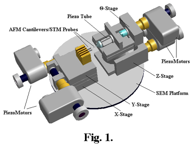
Actuator electrical control signals are conducted through isolated vacuum feedthroughs passing through the SEM main chamber wall. The translation stages share a common electrical circuit, which is often grounded, and the rotating tip and sample holder atop the Z-stage and X-Y stages, respectively, are all connected through the vacuum feedthrough so that the articulating elements can be electrically addressed separately outside the vacuum. Finally, all insulated components and wires are shielded with grounded covers around the SEM observation region to minimize image distortion from charging effects.
As observed with the SEM, the linear stage step sizes are measured to be approximately 4 nm in one direction and 10 nm in the reverse when driven slowly by Picomotor actuators under load. At 1 step/second, the stages require approximately 25 steps to cover a 100 nm distance when driving against the stages' return springs, and 10 steps cover 100 nm in the reverse direction. A single step of a Picomotor momentarily steps the stage between 20 and 30 nm; however, the stage settles back to achieve on average an overall change in distance of 4 nm. Settling appears to stop completely after 3 seconds. As a result of combined loading and actuator characteristics, there is a directional difference in the degree of settling, in that motions opposing the linear stage's return spring display a greater degree of settling. Fewer steps are required to cover the same territory if moving along the force vector of the stage's return spring and if the step period is decreased. This latter effect occurs because the stage has insufficient time to settle back completely as the step frequency rises above 1 Hz. When driven at 1 kHz, the stages travel 25 microns/second smoothly in both directions, thus giving a "dynamic" step resolution of 25 nm. The rotational actuator, which is useful for examining all sides of the tungsten tip and attachments to it, gives angular step sizes of <0.02 degrees with a maximum rotation rate of ~20 degrees/sec.
The piezo tube atop the Z-stage is necessary for continuous motions after the linear stages are brought to within a micron or less of the final desired positions of a manipulation operation. Voltages to the piezo tube supplied by a three-axis controller (Thorlabs) drive the tube to frequencies of up to 10 kHz with translation ranges of several microns. Although no minimum step resolution for the piezo tube could be directly observed, according to noise figures from the piezo driver and accounting for piezo drift and nonlinearities, the spatial resolution of the piezo tube can be estimated conservatively to be under 0.1 nm. For CNT experiments, well-controlled lateral and longitudinal motions are necessary for manipulation and in order to measure, for example, strain-induced conductance properties. Conductivity is typically measured and recorded via a digitizing oscilloscope in two ways; a time-varying voltage is applied to the CNT or contact of interest and current is measured across a resistor in series with the circuit, or a constant voltage is applied across the CNT and current measured while the piezo tube is dithered spatially with a time-varying voltage.
Experimental
MWNTs synthesized by the arc discharge method and purified by oxidation in air were used in some of the experiments, while SWNTs are used in others. The diameters of the MWNTs range from ~2 to 50 nm, with lengths up to 10 µm.16 Atomic force tips with rigid cantilevers for noncontact mode AFM (TESP and FESP models from Digital Instruments) and soft cantilevers for contact mode AFM (CSCS12 model from NT-MDT) were used, along with electrochemically etched tungsten and mechanically sharpened gold and platinum-iridium tips. AFM tips were mounted opposite the rotating tungsten probe tip, which also served as a mount for an AFM cantilever when "dueling" AFM tips were used. The AFM cantilevers were coated with gold to make them more conductive.
Attaching a CNT bundle to an AFM or Scanning tunneling microscope (STM) tip is always the first step; it is done by a rather straightforward process. A visible quantity of purified CNT material is loaded onto a Tungsten or PtIr tip and placed into the tip holder on the x-y stage along with three to six other tips ready for CNT attachment. The AFM or STM tip on the piezo can then be brought into proximity of the raw material. When the tip is brought close enough to a protruding CNT, it "jumps" to the tip and is held in place through van der Waals attraction. The initial jump to the tip could be due to an electrostatic attraction as the elements are being unequally charged with the electron beam or from van der Waals forces. The Van der Waals forces are then sometimes enough to hold the tube and tip together as the tip is pulled from the bunch. If not, a stronger bond can be made using the electron beam to perform localized electron impact-induced dissociation and deposition of the gases present in the chamber, a process which we refer to as "nano-welding." The SEM-nanowelding technique is used to grow a carbonaceous blob of material which acts as a glue.17,18 Figure 2a shows a tip being extracted from the bunch. This tip already has two short tubes attached to it demonstrates not only the extraction procedure but tube to tube attachment as well. The long tube being extracted has been attached to these short tubes by the above mentioned SEM-nanowelding technique.
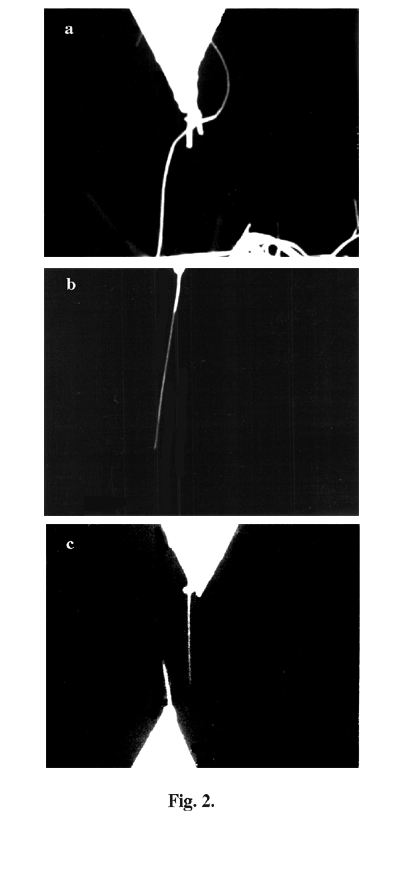
It has been found to be just as easy to attach a CNT to another CNT as it is to attach one to a tip. Though attaching CNTs to AFM tips has been shown previously,16 our technique, attachment with simultaneous viewing under the SEM, allows the CNT tip to be inspected and immediately altered if desired. Usually the first extracted element is not an individual CNT, but a bundle as is shown in Figure 2b. If a bundle is pulled it can then be brought to another of the loaded tips and pulled or burned in two leaving sharp CNTs attached to two tips. It is believed that such a bundle has been attached to the tip in Figure 2b as it is clearly seen to widen for a short segment of its length. The free end of this tube was then attached to another AFM tip and "burned" in two by running 30 microamps of current through it. The resulting two tubes attached to their respective AFM tips are shown in Figure 2c. The tips have not been moved after the burning showing that the tube did not cleave across it's length, but along it, indicating that the tube was likely a bundle which is now delaminated into separate tubes.
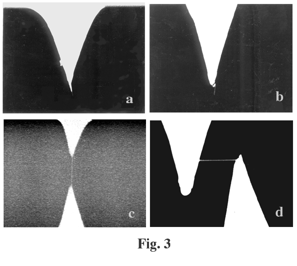
Attaching tubes at both ends to two individually articulated elements is done in the same manner for the stressing experiments. Also shown in Figure 3 are images with a CNT attached to an AFM tip (a), a strange-shaped CNT attached to an AFM tip (b), a CNT link between ends of AFM tips (c) and a CNT link between sides of AFM tips (d). Attaching a short nanotube especially SWNT on AFM or STM tip is essential for the thus gotten AFM or STM nanotube tip to be useful as a perfect probe in AFM or STM imaging as well as serve as a perfect point contact electrode in electrical measuremnet, because a shorter tube can be more rigid laterally and as a result more stable.
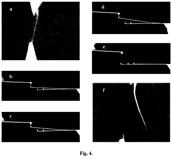
A sequence of images obtained while pulling a CNT bundle is shown in Figure 4. A high magnification image of the tube and its connecting AFM tips is shown in Figure 4a, unfortunately it is not high resolution. This tube has been attached to a stiff AFM cantilever on the left (spring constant 100N/m) and a soft AFM cantilever on the right(spring constant 0.03 N/m). The next three images (4c,4d and 4e), show the softer cantilever's deflection increase as the stiff cantilever is moved in the upward direction. The return to zero deflection is shown in 4e after the tube has broken. Another higher magnification image, Figure 4f, demonstrates that the tube has "broken" near the lower attachment point. Using the AFM cantilevers allows the force to be measured as the tubes are pulled. For this set of images, the total deflection of the softer cantilever (45 microns) gives a calculated breaking force of 1.3 µN. The breaking mechanism is not known. From Figure 4f it is seen that the CNT or bundle thins three times along its length which can be interpreted in two ways. The CNT could have been a single MWNT where the inner shells have been pulled from the outer shells19 or it could have been a bundle of tubes which were delaminated from each other at the breaking point. The resolution of this SEM is not high enough to determine which has actually occurred, though the concentricity of the tube does suggest the former. This phenomenon is known as "sword and sheath" failure and has been observed with much larger carbon fibers.19 Further study is indicated, including TEM imaging of respective parts to show in detail their structure. We plan such work in the near future. Several runs indicate that single tubes are being extracted from bundles during pulling and a bundle which culminates in a very thin tube is a common result after bundles have been pulled apart.
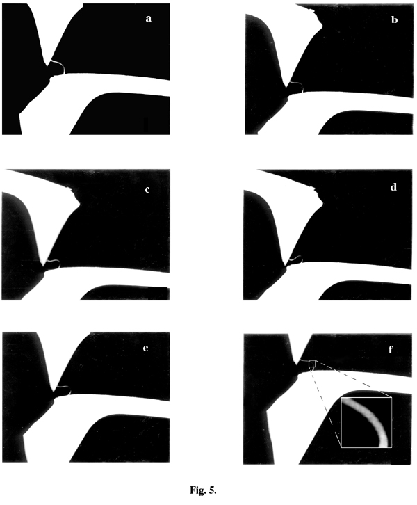
The next set of images (5a to 5f) in Figure 5 shows a CNT or bundle bent by bringing the two AFM levers toward each other. Here the upper cantilever has a force constant of 17 N/m and the bottom tip one of 0.03 N/m. Figure 5 show the tube changes as the upper tip is moved in the downward direction. Between Figures 5c and 5d the lower cantilever rebounded a small amount, moving upward. This indicates that a stress-releasing "kink" may have formed in the tube at this high bending stress. The maximum deflection of the lower lever is 2 microns while the maximum CNT deflection was 0.5 microns. Taking the diameter of the CNT to be 50nm (which we have not accurately measured) and the length to be 1 micron the calculated lower limit of Young's modulus for this CNT is 100GPa. Figures 5e and 5f are taken as the upper tip is retracted in the upward direction. This tube did not return to its original shape after retraction and was thus irreversibly changed by the bending. Other tubes, though are more resilient, returning to their original shape after repeated bending and buckling, they were done with SWNT material and are thus more likely isolated single walled tubes. A more resilient, elastic tube is shown along with other experiments including lateral bending, kinking, and tensile-loading leading to breakage in a video presentation included at this site: nanobridge.mov, nanohook.mov, nanoswitch.mov. [QuicktimeTM (or an alternative movie player) is required to view the movies. QuicktimeTM can be downloaded from http://www.apple.com/quicktime/]
Conductivities can be measured between the AFM/STM tips since they are independently connected via electrical feedthroughs to the outside of the SEM vacuum chamber. Figure 6 contains SEM images of CNT connections (left) and corresponding electrical traces (right). The circuit used to obtain all traces shown here is a simple voltage divider where the CNT is in series with a resistor (270 kOhm). A triangle wave, shown in all traces, is applied across the entire circuit while the voltage across the resistor is recorded. Figure 6a shows a nanotube tangle contacting a conductive tip. The tangle touches at several points on the lower side of the tip, and the corresponding electrical behavior of this connection is shown as rectifying. In this instance, the tube conducts predominantly in one direction; however, rectification has been observed for both polarities. Figure 6b shows a nanotube-to-nanotube contact and its electrical trace. Here the long nanotube is drawn away via van der Waals from the tangle by a short nanotube attached to the tip. The conductivity is non-linear with driving voltage and small in magnitude. Conduction is apparently limited by the nanotube crossing junction, which is very nearly a perfect point contact. Further investigations are planned to explore the utility of this technique to probe nanotube sidewall defects.
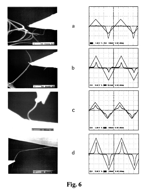
Figure 6c shows a stressed nanotube connected between a gold-coated AFM tip (upper) and the conductive surface of an AFM cantilever (lower). The originally straight nanotube was attached to the AFM tip via SEM-nanowelding and then brought down to the back of the cantilever and compressed until the tube deformed into the curve shown. The conductivity trace for figure 6c shows an interesting deviation from most of the conductivity curves observed in these experiments. This behavior may be stress-related, since it appeared as the tube underwent bending, but it might also be a consequence of the contact geometry of the end of the nanotube on the back of the gold-coated cantilever. Figure 6d shows a long multiwall nanotube connected between a tungsten STM tip (upper) and a gold-coated AFM tip (lower). The trace shown in 6d is a typical conductivity signature; the most common behavior is of a non-linear semiconductive I-V character. Occasionally a CNT will be singled out and display no conductivity with more than a 10 volt potential applied. High conductivity ohmic behavior, in which the current linearly reflects exactly the driving waveform, is also observed. A perfect rectification trace is found infrequently and rectification can be permanently eliminated by applying too much voltage, resulting either in a broken contact or fully conductive curve. Changes from semiconductive character to fully conductive are also observed when the applied voltage is high enough. It is too early to conclude whether this behavior is fundamental to the CNT or to the contact junction of the tube and tip. In order to explore contact effects, several experiments were performed to test tip-to-tip conductivities, where similar traces were obtained. This demonstrates that care must be exercised to remove contact effects, especially when the tube is placed under stress and contact geometries may change as a result.
Discussion
The above experiments demonstrate the capability of the nanomanipulator inside an SEM as a construction device and as a test bed for nanoscale materials. Selection and attachment of CNTs with real time viewing and real time mechanical and electrical testing is a start at constructing more complex CNT devices. We find the free space manipulations more fruitful than work we have done using the atomic force microscope for pushing and bending of CNTs lying on surfaces. AFM manipulation is two-dimensional, not in real-time, and restricted to the sample surface. Nanomanipulation under an SEM is not limited by any of the above AFM restrictions and can be done without sacrificing any of the positional resolution.
Attaching CNTs to AFM cantilevers has been shown to improve AFM imaging resolution and we have shown another route to their production that further allows simultaneous high resolution inspection and immediate modification. These tips should prove useful for AFM imaging, or as adequate conductivity is verified in the nanomanipulator, for AFM field-induced oxidation lithography.20 As the x-y stage allows 6mm of travel, several tips can be loaded at once for batch production with our current throughput of about three tips per hour. The resilience of the CNT demonstrates that these tips will withstand abuse in the AFM without suffering catastrophic failure of the tube or the tube to tip attachment. Transferring tubes from tip to tip is occasionally accomplished by progressively stronger van der Waals attraction via larger contact area, but SEM-nanowelding is used more commonly, ensuring a stronger attachment. After a weak deposited joint has been made by SEM-nanowelding, components can be transferred by creating a stronger bond elsewhere and slipping the tube out of or breaking via shear force movements the previous weld. Attaching both ends of a CNT bundle to separate AFM tips and then pulling them apart usually results in two CNT AFM tips which both culminate with single tubes.
The mechanical experiments on CNTs thus far have shown them to be strong and elastic as predicted. the tubes that show irreversible mechanical strains are more likely bundles of tubes which slide relative to each other and are then held in these new contorted geometry by the strong van der Waals attraction between tubes. Both reversible and irreversible mechanical properties might find use in larger CNT structures. The ability to identify a tube's or bundle of tube's behavior before incorporation into large assemblies will be very important and the nanomanipulator is well suited as a test-bed and assembly device for such strctures. Electrical properties, specifically mechanically inducaed electrical effects, will be studied more carefully. Attaching CNTs to electrical contacts along their length as well as just at the CNT tip may give different electrical behaviors. The SEM nanomanipulator allows investigations where the electriacl conatct can be purposefully formed along a specified lenght of tube or at the tube end so that the contact area is well known. These contacts and tubes can then be stressed mechanically whilw simultanenously monitoring electrical behavior such that bends and kinks in tubes can be correlated with electrical properties.
Summary
A nanomanipulator within an SEM has been successfully developed. The nanomanipulator is capable of large travel as well as nanometer final translation resolution in three dimensions and one axis of rotation. The versatility of the nanomanipulator was tested using CNTs as the manipulation object. CNTs have been attached to AFM tips allowing the applied forces to be measured while mechanically stressing the tubes. Electrical connections to the separate articulating components allow conductivity to be monitored while the mechanical stressing occurs. Bending, kinking, and breaking of nanotubes or nanotube bundles has been accomplished showing the manipulator to be a useful test-bed for investigating the mechanical and electrical properties of nanosize materials. The manipulator has been shown to be useful for picking, placing, and attaching nanosize components with the ultimate goal of assembling useful nanoscale devices from pre-fabricated elements.
References
- J. W. Mintmire, B. I. Dunlap, and C. T. White, Phys. Rev. Lett.68, 631 (1992).
- N. Hamada, S. I. Sawada, and A. Oshiyama, Phys. Rev. Lett.68, 1579 (1991).
- T. W. Ebbesen, H. J. Lezec, H. Hiura, J. W. Bennett, H. F. Ghaemi, and T. Thio, Nature382, 54 (1996).
- J. W. G. Wildoer, L. C. Venema, A. G. Rinzler, R. E. Smalley, and C. Dekker, Nature391, 59 (1998).
- S. J. Tans, M. H. Devoret, H. J. Dai, A. Thess, R. E. Smalley, L. J. Geerligs, and C. Dekker, Nature386, 474 (1997).
- M. Bockrath, D. H. Cobden, P. L. McEuen, N. G. Chopra, A. Zettl, A. Thess, and R. E. Smalley, Science275, 1922 (1997).
- S. Frank, P. Poncharal, Z. L. Wang, and W. A. d. Heer, Science280, 1744 (1998).
- S. J. Tans, A. R. M. Verchueren, and C. Dekker, Nature393, 49 (1998).
- G. Overmey, W. Zhong, and D. Z. Tomanek, Phys. D27, 93 (1993).
- B. I. Yakobson, C. J. Brabec, and B. J, Phys. Rev. Lett76, 2511 (1996).
- M. M. J. Treacy, T. W. Ebbesen, and J. M. Gibson, Nature381, 678 (1996).
- E. W. Wong, P. E. Sheehan, and C. M. Lieber, Science277, 1971 (1997).
- B. I. Yakobsen, M. P. Campbell, C. J. Brabec, and J. Bernholc, Comput. Mater. Sci.8, 341 (1997).
- T. Hertel, R. Martel, and P. Avouris, J. Phys. Chem. B102, 910 (1998).
- R. S. Ruoff, J. Tersoff, D. C. Lorents, S. Subramoney, and B. Chan, Nature364, 514 (1993).
- J. H. Hafner, Nanotube tips for AFM at http://cnst.rice.edu/mount.html.
- N. Miura, H. Ishii, J. I. Shirakashi, A. Yamada, and M. Konagai, Appl. Surf. Sci.113/114, 269 (1997).
- H. W. P. Koops, J. Kretz, M. Rudolph, M. Weber, G. Dahm, and K. L. Lee, Jpn. J. Appl. Phys., Part 133, 7099 (1994).
- M. S. Dresselhaus, D. Dresselhaus, K. Sugihara, I. L. Spain, and H. A. Goldberg, Graphite Fibers and Filaments(Apringer-Verlag, New York), P151.
- P. Avouris, R. Martel, T. Hertel, and R. Sandstorm, Appl. Phys. A66, 659 (1998).
|