Simple Fabrication of Nanoscale Metal Interconnects
W.J. Dressick, M-S. Chen, and S.L. Brandow*
Code 6950, Center for Bio/Molecular Science and Engineering, Naval Research Laboratory,
Washington, DC 20375-5348 USA
This is an abstract
for a presentation given at the
Eighth
Foresight Conference on Molecular Nanotechnology.
There will be a link from here to the full article when it is
available on the web.
Nanotechnology is concerned with the development of the materials and procedures required for assembly, in an atom-by-atom fashion, of novel structures having unique properties or capabilities. However, in many cases, the ability to utilize such structures successfully will require an interface to the macroscopic world. For example, nanoscale computers, whatever their architecture, will certainly require some means of power and communication with the user. Conventional nanolithography techniques, spanning the size realm of ~10-100 nm, offer one possibility for fabricating such connections. In particular, we have been investigating molecular self-assembly processes [1], in conjunction with proximal probe or electron-beam patterning techniques [2-4], to facilitate fabrication of conductive metal interconnects at these dimensions.
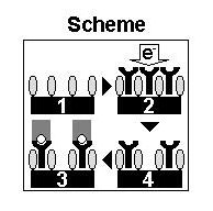
One example of the general type of process [5, 6] we have examined is illustrated in the Scheme. Solution chemisorption of an aromatic trichlorosilane first creates a polysiloxane self-assembled monolayer (SAM) film (ellipses) bearing well-defined nanocavities on the surface of a substrate (panel 1). Subsequent adsorption of a metal-binding ligand material (wrench structures) into the nanocavities (panel 2) prepares the SAM for patterning. Patterned exposure of the SAM using a high-energy electron-beam [6] displaces or degrades the entrapped ligand, creating a nanopatterned reactivity template in the SAM (panel 3). Treatment of the patterned SAM with a Pd nanoparticle catalyst dispersion (circles) [6-8] selectively binds Pd metal only at intact ligand sites in the SAM (i.e., positive-tone imaging). Subsequent immersion of the catalyzed substrate in an electroless metal bath deposits a metal film (rectangles) only at the catalyzed sites, creating a nanoscale metal pattern (panel 4). In this manner, features in metal with linewidths to ~50 nm can be fabricated with adequate critical dimension control. The process is carried out primarily under aqueous conditions, mitigating environmental and waste disposal concerns. Our presentation will focus on the details and permissible variations of the process, including SAM, exposure, and catalyst parameters that influence the quality and ability to control critical dimensions of the metal features.
References:
- W.J. Dressick and J.M. Calvert, Jpn. J. Appl. Phys. 32, 5829 (1993).
- F.K. Perkins, et al., Appl. Phys. Lett. 68, 550 (1996).
- S.L. Brandow, et al., J. Vac. Sci. Tech. A 15, 1455 (1997).
- S.L. Brandow, et al., J. Vac. Sci. Tech. B 15, 1818 (1997).
- W.J. Dressick, et al., J. Amer. Chem. Soc. 122, 982 (2000).
- S.L. Brandow, et al., Appl. Phys. Lett., submitted.
- W.J. Dressick, et al., Coll. Surf A 108, 101 (1996).
- S.L. Brandow, et al., J. Electrochem. Soc. 144, 3425 (1997).
*Corresponding Address:
Susan Brandow
Code 6950, Center for Bio/Molecular Science and Engineering, Naval Research Laboratory
4555 Overlook Ave.
Washington, DC 20375-5348 USA
Email: [email protected]
|