SET device using self-assembled monolayers
in a planar nanoelectrode arrangement
J.M. Köhler*, a, A. Csákia, Th. Wagnerb, W. Krechb, J. Fuchsc, U. Hübnerc, W. Fritzschea
aInst. for Physical High Technology,
Jena, Thuringia D-07745 Germany
bInst. for Solid State Physics, Jena
bInst. for Applied Physics, Jena
This is an abstract
for a presentation given at the
Eighth
Foresight Conference on Molecular Nanotechnology.
There will be a link from here to the full article when it is
available on the web.
The investigations reported here are to understand as a contribution for bridging (bio)molecular processes and chip technologies at the level of single particle management. The control of tunneling of a single electron ("SET") is well known in inorganic systems. The electron transport control is realized in these devices by the capacitive application of an electrical field to a nanofabricated metallic thin film element, an electronic confinement, which is coupled with two electrical conductors by tunneling barriers [1-3]. The barriers are built-up by electrical insulators like Al2O3 and possess a thickness in the range of about 2 nm. If one electron has passed the tunneling barrier, the tunneling probability for a second electron is changed by the charge of the first one, that means the electron transport to or from the confinement is controlled by Coulomb effect. The SET-effect depends on the size of electronic confinement. It is lowered by thermal excitation and was normally found in the sub-1K-region. It was shown for example in so-called SAIL contacts up to temperatures of 4K.
The barrier for electron tunneling should be much more precisely designed in case of barriers with well defined thickness and electron transport properties. Therefore, molecular monofilms of organic or biomolecules should be more suited for the construction of a SET-barrier than oxide films. In addition, such monofilms offer two interesting possibilities: (1) It is possible to incorporate single molecules of one type in a matrix of an other in order to study electron transport properties of single molecules in a metallic surrounding. (2) Intramolecular electron confiments should be realized in addition to metallic nanoconfinements. The geometry of arrangement is much better defined than in STM experiments and compatibel to the chip technology.
We investigated the introduction of an alkylthiol-monolayer in a self-aligned in-line SET transistor (SAIL technology) as a model for the single electron transport behaviour of biomembranes and synthetic molecular films between metallic electrodes. For the preparation we use the well known self-assembling activity of the thioles at Au surfaces. At first we tested n-octylthiol. Two nanofabricated Au electrodes on a silicon chip were covered by C8H17SH from ethanolic solution by incubation at about 5oC for 3 hrs. The alkylthiol forms a self assembled monolayer (SAM). After this, a second Au layer (thickness 70 nm) was deposited by low energy sputtering onto the SAMs and nanopatternd by lift-off using a mask previously written by electron beam lithography.
Electrical measurements were performed at 0.3 K and 4.2 K. They show, that the molecular monofilm is suited for SET barriers as well as the known inorganic films. The current-voltage characteristics is typical for the Coulomb blockade. Additionally, the influence of a capacitively coupled electrical field was studied in order to modulate the electron transport periodically in dependence of the gate voltage which was applied by a third Au nanoelectrode. We observed a strong oscillatoric modulation of the source-drain current in dependence of gate voltage as a safe criterion for the control of single electron transport by the capacitive coupled nanoelectrode (Fig. 1). The modulation periode amounts to about 30 mV. That agrees well with the expected values. This means, that the layer of alkyl residues is working as an efficient tunneling barrier for the electron transport.
The diode I/U plot as well as the transistor I/U plot show a superposed modulation signal in addition to the main current extremas. Such a pattern is unknown from inorganic tunneling barriers. It is supposed, that this pattern is connected with intermediate states in the electron transport through the molecular film. It is thinkable, that the molecular asymmetry could be responsible for the effect, which is caused by the head/tail construction of the amphiphilic molecules.
References
- Single Charge Tunneling: Coulomb Blockade Phenomena in Nanostructures, ed. By H. Grabert and M.H. Devoret (Plenum, New York 1991)
- T.A. Fulton and G. J. Dolan: Phys. Rev. Lett 59 (1987), 109
- M. Götz et al.: J. Appl. Phys. 78 (1995), 5499
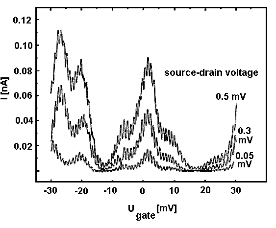 |
| Fig. 1. Current through a nanofabricated alkylthiol monolayer double junction with Au nanoconfinement in a SAIL SET transistor in dependence of gate voltage for three different source drain voltages (50 �V, 0.3 mV and 0.5 mV) |
*Corresponding Address:
J. Michael Koehler
Institute for Physical High Technology
Winzerlaer Str. 10
Jena, Thuringia D-07745 Germany
Email: [email protected]
|