Copper Nanowire Molecular Electronics Network with 10 nm Wide Cu Nanowire Interconnects
R. Adelung*, a, A. Scottc, F. Ernsta, L. Kippb, M. Skibowskib , and M. Tabib-Azarc
aDepartment of Material Science and Engineering, Case Western Reserve University,
Cleveland, Ohio 44106-7204 USA
bInstitut für Experimentelle und Angewandte Physik, Christian Albrechts Universität zu Kiel, Germany
cDepartment of Electrical Engineering and Computer Science, Case Western Reserve University,
Cleveland, Ohio, USA
This is an abstract
for a presentation given at the
Ninth
Foresight Conference on Molecular Nanotechnology.
There will be a link from here to the full article when it is
available on the web.
In the last few years it was shown that nanowire networks consisting of the alkali metal Rb can be formed on layered crystal surfaces [1]. In a self-organized manner, macroscopic networks (cm scale) of thin (5-250nm) metallic wires with a micron scale mesh size are formed within minutes of evaporation. The Rb metal was evaporated from a dispenser source in ultra high vacuum (UHV) [2]. These networks have been useful in characterizing some general features of low dimensional crystals [3,4], however Rb wires are immediately oxidized in air.
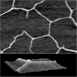
Recent experiments show that nanowire networks consisting of copper can be obtained in a similar manner [5]. Evaporation of copper onto cleaved VSe2 surfaces also leads to a self-organized process described in [5], which ends in the formation of nanowire networks. In this presentation, we discuss AFM measurements in air that we used to find out details about the characteristics of the Cu nanowires. We show that copper nanowire networks are a good choice for molecular electronics network by considering the aspect ratios of these wires and the geometry of "Y" junctions between different arms of the nanowire. The cross points of the nanowires stand up like one-dimensional tips (see figure, baseline dimension of the upper image: 1500nm, lower image is a three dimensional representation of an magnification of the upper image), which might be utilized for contacts between different layers formed at the top of each other. Moreover, a large variation in the mesh size can be obtained by changing the evaporation conditions. Therefore a suitable substrate area can be customized for research like diffusion studies or molecular crystal growth behavior. Terminating the nanowire growth in an early state results in an open network with many nanowire ends. We present different AFM scans showing the variety of accessible geometries and first experiments combining nanowire networks and organic molecules (rotaxanes and dodecanethiol).
References:
- R. Adelung, L. Kipp, J. Brandt, L. Tarcak, M. Traving, C. Kreis, and M. Skibowski, Appl. Phys. Lett. 74, 3053(1999).
- Rb dispenser from SAES Getters, Lainate (Milano), Italy.
- R. Adelung, J. Brandt, K. Roßnagel, O. Seifarth, L. Kipp, M. Skibowski, C. Ramirez, T. Strasser, and W. Schattke: Phys. Rev. Lett. 86, 1303 (2001)
- R. Adelung, J. Brandt, L. Kipp and M. Skibowski, Phys. Rev. B. 63, 165327 (2001)
- R. Adelung, F. Ernst, M. Tabib-Azar et al., in preparation
Abstract in RTF format 6,756 bytes
*Corresponding Address:
R. Adelung
Department of Material Science and Engineering, Case Western Reserve University
10900 Euclid Avenue, Cleveland, Ohio 44106-7204 USA
Phone: (216) 368 4214
Fax: (216) 368 3209
Email: [email protected]
|