Electrical and Mechanical Characterization of Embedded Metal Nanocrystals by Microelectronic-Based Test Structures
School of Electrical and Computer Engineering, Cornell University,
Ithaca, NY 14853 USA
This is an abstract
for a presentation given at the
Ninth
Foresight Conference on Molecular Nanotechnology.
There will be a link from here to the full article when it is
available on the web.
Nanometer-scale metal layers and clusters (or commonly referred to as nanocrystals) play an important role in organic and inorganic nanotechnology in formation of special device structures such as metal-gate CMOS (Lu 2000), nonvolatile memory (Liu 2000), and carrier injector at material interface (Abkowitz 1998, Tadayyon 1999, Narayanan 2000). They are also commonly used as the growth base of organic self-assembled monolayers (SAM) and nanotubes for catalytic or registration purposes. With the form factor ranging from 1-50nm, though the metal clusters can be internally defect-free (hence the name nanocrystal), the atomic site arrangement on the surface can deviate significantly from the bulk lattice as a result of total energy minimization during the formation process (Suo 1998). There are still a significant number of atoms in the cluster ranging from 100 to millions, and hence the valence electron screening can mostly be viewed mesoscopically. It is a common conjecture that the size effect on electrical and mechanical properties of metal clusters will only be significant toward or below the 1nm scale. However, lack of reliable measurement methods in that scale poses severe limits on applying accurate parameter calibration for models derived from theoretical studies.
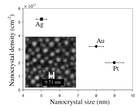
In this work, we will present current-voltage and capacitance-voltage measurement results for metal nanocrystals embedded in insulators and bulk metal/semiconductor interface in MOS capacitors, floating-gate MOSFET, and Kelvin contact structures. Morphology and size can be indirectly extracted from the charging asymmetry (cluster formation), Coulomb blockade (cluster self and cross capacitance) and flat-band voltage shift (surface sparsity and average volume). Surface adhesion and diffusivity can be extracted from annealing temperature profiles and subsequent retention lifetime characteristics. Work function can be correlated to charge injection efficiency. Although these characterization methods are mostly indirect and limited to embedded clusters, our microelectronic-based test structures are more sensitive and reproducible in some aspects and provide supplemental information comparing to physical measurement from SEM/TEM/STEM.
References:
- Abkowitz M., Facci J. S., Rehm J. (1998): J. Appl. Phys., vol. 83, no. 5, pp. 2670-2676. Direct evaluation of contact injection efficiency into small molecule based transport layers: influence of extrinsic factors.
- Lu Q., Yeo Y. C., Ranade P., Takeuchi H., King T.-J., Hu C., Song S. C., Luan H. F., Kwong D. (2000): Proc. Symp. VLSI Technology, pp. 72-73. Dual-metal gate technology for deep-submicron CMOS transistors.
- Liu Z., Kim M., Narayanan V., Kan E. C. (2000): Superlattice and Microstructures, vol. 28, no. 5/6, pp. 393-399. Process and device characteristics of self-assembled metal nano-crystal EEPROM.
- Narayanan V, Liu Z., Shen Y. N., Kim M., Kan E. C. (2000): IEDM Tech. Dig., pp. 365-368. Reduction of metal-semiconductor contact resistance by embedded nanocrystals.
- Suo Z., Zhang Z. (1998) Phys. Rev. B, vol. 58, pp. 5116-5120.
- Tadayyon S. M., Griffiths K., Norton P. R., Tripp C., Popovic Z. (1999): J. Vac. Sci. Technol. A, vol. 17, no. 4, pp. 1773-1778. Work function modification of indium-tin-oxide used in organic light emitting diodes.
Abstract in RTF format 8,484 bytes
*Corresponding Address:
Edwin C. Kan
School of Electrical and Computer Engineering, Cornell University
404 Phillips Hall, Ithaca, NY 14853 USA
Phone: 607-255-3998
Fax: 607-254-4565
Email: [email protected]
http://www.ece.cornell.edu/~kan
|