Electronic Rectification, Ballistic Switching, and Logic Functions with Carbon Nanotube `Y-Junctions'
D Srivastava*, a, A Andriotisb, M Menonc, L Chernozetonskid
aComputational Nanotechnology, NASA Ames Research Center,
Moffett Field, CA 94035-1000 USA
bInstitute of Electronic Structure, FRT-Hellas, Crete, Greece
cCenter for Comp. Sciences, U of Kentucky, Lexington, KY, USA
dInst. of Biochem. Phys., Russian Acad. Sc., Moscow, Russia
This is an abstract
for a presentation given at the
Ninth
Foresight Conference on Molecular Nanotechnology.
There will be a link from here to the full article when it is
available on the web.
Carbon nanotubes and nanotube heterojunctions have recently been proposed as excellent candidates for nanoscale molecular electronic device components, nano-electromechanical and nano-electrochemical sensors and machines. It is well known that carbon nanotubes, hollow cylindrical structures made of sheets of carbon atoms, are both metallic and semiconducting. Initial experiments and theory suggested their use in nanoscale quantum molecular wires with excellent current carrying capacity. Two terminal heterojunctions of nanotubes of semiconducting and metallic nature have been proposed as model of nanoscale rectifying switches, and this behavior has been verified in experiments as well.[1,2]
For any current based architecture for nanotube based electronics to work, three terminal nanoscale devices and nanotube junctions are essentially required. Such junctions can be introduced and have been proposed in the form of carbon nanotube "T-" and "Y-junctions." [3] The three terminal multi-wall "Y" junctions have also been synthesized in recent experiments, and electronic transport using the "Y" junction as a two-terminal device show asymmetric and rectifying I-V characteristics. [4,5]
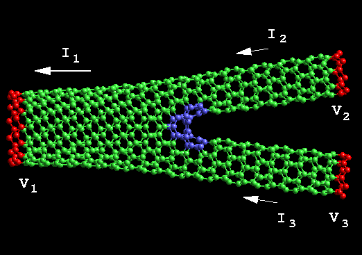
I-V characteristics of single-wall carbon nanotube Y-junctions are calculated using an efficient embedding Green's Function formalism that allows for conductance across nanotube multiple junctions and realistic nanotube metal-lead contacts. The current vs voltage characteristics show the asymmetry and rectification, in agreement with recent experimental results on multiwall nanotube Y-junctions. [6] In symmetric Y-nanotube junctions the rectification has a weak dependence on the angle at the junction, and can support both ballistic rectification and/or ballistic switching operating modes. Although structural symmetry of the Y-junction is found to be necessary condition for ballistic rectification, it may not be sufficient for all cases. [7] Transport calculations as a 3-terminal device show modulation of the current in the bias channel and a branch as a fucntion of applied voltage across the other branch. This behavior can be exploited to propose simple logic functions with current flowing across carbon nanotube Y junctions.
References:
- P. Collins and P. Avouris, Scientific American, pg. 62, December 2000 issue for a general review article in this area.
- Z. Yao et al., Nature, Vol 402, 273 (1999)
- M. Menon and D. Srivastava, Phys. Rev. Lett. Vol 79, 4453, (1997); M. Menon and D. Srivastava, J. Mat. Res. Vol 13, 2357 (1998)
- C. Papadopoulos et. al., Phys. Rev. Lett. Vol. 85, 3476 (2000)
- C. Satishkumar et. al., Appl. Phys. Lett. Vol. 77, 2530 (2000)
- A. Andriotis, M. Menon, D. Srivastava, and L. Chernozetonski, Phys. Rev. Lett., to appear (2001)
- A. Andriotis, M. Menon, D. Srivastava and L. Chernozetonski, Appl. Phys. Lett. to appear (2001)
*Corresponding Address:
D Srivastava
Computational Nanotechnology, NASA Ames Research Center,
MS T27A-1, Moffett Field, CA 94035-1000 USA
phone: 650-604-3486
fax: 650-604-3957
email: [email protected]
http://www.nas.nasa.gov/~deepak/home.html
|