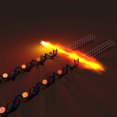
The “molecular threading” technique disclosed by Aeon Biowares that was the topic of our previous post was presented as a great improvement over earlier bulk methods for stretching DNA, such as “molecular combing”, and the researchers speculated that it might also be useful for fabricating arrays of nanowires. As a starting point to thinking about what molecular threading might make possible, it might be useful to consider what current methods like molecular combing can accomplish. A hat tip to Josh Hall for pointing to this example of what can already be done in terms of using DNA strands to assemble functional arrays “Stanford scientists use DNA to assemble a transistor from graphene“.
DNA is the blueprint for life. Could it also become the template for making a new generation of computer chips based not on silicon, but on an experimental material known as graphene?
That’s the theory behind a process that Stanford chemical engineering professor Zhenan Bao reveals in Nature Communications [abstract]. …
Graphene has the physical and electrical properties to become a next-generation semiconductor material – if researchers can figure out how to mass-produce it.
Graphene is a single layer of carbon atoms arranged in a honeycomb pattern. Visually it resembles chicken wire. Electrically this lattice of carbon atoms is an extremely efficient conductor.
Bao and other researchers believe that ribbons of graphene, laid side-by-side, could create semiconductor circuits. Given the material’s tiny dimensions and favorable electrical properties, graphene nano ribbons could create very fast chips that run on very low power, she said.
“However, as one might imagine, making something that is only one atom thick and 20 to 50 atoms wide is a significant challenge,” said co-author Sokolov.
To handle this challenge, the Stanford team came up with the idea of using DNA as an assembly mechanism.
Physically, DNA strands are long and thin, and exist in roughly the same dimensions as the graphene ribbons that researchers wanted to assemble.
Chemically, DNA molecules contain carbon atoms, the material that forms graphene.
The real trick is how Bao and her team put DNA’s physical and chemical properties to work.
The researchers started with a tiny platter of silicon to provide a support (substrate) for their experimental transistor. They dipped the silicon platter into a solution of DNA derived from bacteria and used a known technique to comb the DNA strands into relatively straight lines.
Next, the DNA on the platter was exposed to a copper salt solution. The chemical properties of the solution allowed the copper ions to be absorbed into the DNA.
Next the platter was heated and bathed in methane gas, which contains carbon atoms. Once again chemical forces came into play to aid in the assembly process. The heat sparked a chemical reaction that freed some of the carbon atoms in the DNA and methane. These free carbon atoms quickly joined together to form stable honeycombs of graphene.
“The loose carbon atoms stayed close to where they broke free from the DNA strands, and so they formed ribbons that followed the structure of the DNA,” Yap said.
So part one of the invention involved using DNA to assemble ribbons of carbon. But the researchers also wanted to show that these carbon ribbons could perform electronic tasks. So they made transistors on the ribbons.
“We demonstrated for the first time that you can use DNA to grow narrow ribbons and then make working transistors,” Sokolov said.
The paper drew praise from UC Berkeley associate professor Ali Javey, an expert in the use of advanced materials and next-generation electronics.
“This technique is very unique and takes advantage of the use of DNA as an effective template for controlled growth of electronic materials,” Javey said. “In this regard the project addresses an important research need for the field.”
Bao said the assembly process needs a lot of refinement. For instance, not all of the carbon atoms formed honeycombed ribbons a single atom thick. In some places they bunched up in irregular patterns, leading the researchers to label the material graphitic instead of graphene.
Even so, the process, about two years in the making, points toward a strategy for turning this carbon-based material from a curiosity into a serious contender to succeed silicon.
“Our DNA-based fabrication method is highly scalable, offers high resolution and low manufacturing cost,” said co-author Yap. “All these advantages make the method very attractive for industrial adoption.”
This paper demonstrates using DNA molecules aligned and stretched by molecular combing to bind copper ions, which act as catalysts of chemical vapor deposition for the growth of graphitic (that is, they contained both sp2 and sp3 carbon atoms) nanoribbons less than 10 nm in width and more than 20 µm in length. The graphitic nanoribbons mimicked the DNA nanostructures used as templates in terms of density, bundling, and branching of strands. In these experiments the only way in which the density, bundling, and branching of these double-strand DNA molecules could be controlled was by DNA concentration and ionic strength. The authors focus on the need to better control reduction of metal ions and growth conditions to yield pristine single-layer graphene nanoribbons. It is also interesting to speculate on what increased complexity of circuitry could results from using molecular threading to arrange DNA templates.
—James Lewis, PhD


