One of the core concepts of molecular manufacturing is that nanotechnology will evolve to the point that it will become possible to position small groups of reactive atoms at atomically precise desired locations on a work piece in order to build arbitrarily complex atomically precise structures. For several decades optical tweezers have been used to trap and manipulate micrometer-size objects, like bacteria, molecules attached to micrometer size beads, and organelles within eukaryotic cells. They have been limited in precision by the wavelength of light (about 400 to 700 nm) so that they have been unable to manipulate nanometer-scale objects. Two recently published papers raise the possibility that this technology might evolve through the use of surface plasmon polaritons to enable atomically precise positioning. One paper presents a theoretical proposal for extending optical trapping to particles smaller than 2 nm. The second presents an experimental demonstration of highly efficient nanofocusing.

To grasp and move microscopic objects, such as bacteria and the components of living cells, scientists can harness the power of concentrated light to manipulate them without ever physically touching them.
Now, doctoral student Amr Saleh and Assistant Professor Jennifer Dionne, researchers at the Stanford School of Engineering, have designed an innovative light aperture that allows them to optically trap smaller objects than ever before – potentially just a few atoms in size.
The process of optical trapping – or optical tweezing, as it is often known – involves sculpting a beam of light into a narrow point that produces a strong electromagnetic field. The beam attracts tiny objects and traps them in place, just like a pair of tweezers.
Unfortunately, there are natural limits to the technique. The process breaks down for objects significantly smaller than the wavelength of light. Therefore, optical tweezers cannot grasp super-small objects like individual proteins, which are only a couple of nanometers in diameter.
Saleh and Dionne have shown theoretically that light passed through their novel aperture would stably trap objects as small as 2 nanometers. The design was published in the journal Nano Letters [abstract], and Saleh is now building a working prototype of the microscopic device. …
Dionne says that the most promising method of moving tiny particles with light relies on plasmonics, a technology that takes advantage of the optical and electronic properties of metals. A strong conductor like silver or gold holds its electrons weakly, giving them freedom to move around near the metal’s surface.
When light waves interact with these mobile electrons, they move in what Dionne describes as “a very well-defined, intricate dance,” scattering and sculpting the light into electromagnetic waves called plasmon-polaritons. These oscillations have a very short wavelength compared to visible light, enabling them to trap small specimens more tightly.
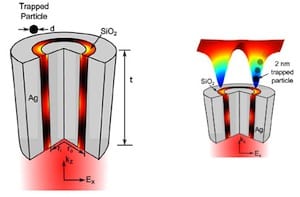
Dionne and Saleh applied plasmonic principles to design a new aperture that focuses light more effectively. The aperture is structured much like the coaxial cables that transmit television signals, Saleh said. A nanoscale tube of silver is coated in a thin layer of silicon dioxide, and those two layers are wrapped in a second outer layer of silver. When light shines through the silicon dioxide ring, it creates plasmons at the interface where the silver and silicon dioxide meet. The plasmons travel along aperture and emerge on the other end as a powerful, concentrated beam of light.
The Stanford device is not the first plasmonic trap, but it promises to trap the smallest specimens recorded to date. Saleh and Dionne have theoretically shown that their design can trap particles as small as 2 nanometers. With further improvements, their design could even be used to optically trap molecules even smaller.
… Saleh is working on turning the design into reality. He hopes to have a prototype by early 2013.
The two obstacles to using optical tweezers to manipulate nanoscale objects are that (1) the diffraction limit to focusing light is about 200 nm, so that (2) smaller particles would require optical intensity high enough to damage the particles. This paper examines the optical force experienced by a dielectric particle interacting with the field scattered by a coaxial plasmonic aperture designed to trap particles at the surface rather than inside the aperture. By considering coaxial apertures with both straight and tapered channels, the authors’ calculations show that optical trapping of dielectric particles as small as 2 nm is possible in both water and air. Furthermore, less than 100 mW optical power would be required, overcoming the second obstacle.
How precisely should it be possible to position a 2 nm particle using the proposed coaxial aperature? Figure 7 of the paper seems to suggest to my non-expert eye that the obtainable precision would be about 8 nm in the x direction and 40 nm in the y direction. If so, achieving atomically precise positioning would require an improvement of about two orders of magnitude. The estimated current precision would, however, be close to what would be necessary to position some types of molecular building blocks.

… Caltech researchers, co-led by assistant professor of electrical engineering Hyuck Choo, have built a new kind of waveguide—a tunnellike device that channels light—that gets around this natural limit. The waveguide, which is described in a recent issue of the journal Nature Photonics [abstract], is made of amorphous silicon dioxide—which is similar to common glass—and is covered in a thin layer of gold. Just under two microns long, the device is a rectangular box that tapers to a point at one end.
As light is sent through the waveguide, the photons interact with electrons at the interface between the gold and the silicon dioxide. Those electrons oscillate, and the oscillations propagate along the device as waves—similarly to how vibrations of air molecules travel as sound waves. Because the electron oscillations are directly coupled with the light, they carry the same information and properties—and they therefore serve as a proxy for the light.
Instead of focusing the light alone—which is impossible due to the diffraction limit—the new device focuses these coupled electron oscillations, called surface plasmon polaritons (SPPs). The SPPs travel through the waveguide and are focused as they go through the pointy end.
Because the new device is built on a semiconductor chip with standard nanofabrication techniques, says Choo, the co-lead and the co-corresponding author of the paper, it is easy integrate with today’s technology.
The new wave guide is expected to be useful for applications in imaging, computer hard drives, and communications. As reported in the research paper, optimal tapering angles and lengths were found through computational simulations. A silicon dioxide dielectric layer measures 200 by 500 nm at the wide end and tapers down to 80 nm by 14 nm at the tip. The upper and lower surfaces were covered with a gold layer about 50 nm thick. The device was fabricated using electron beam-induced deposition, focused ion-beam milling, and electron-beam evaporation. A two-photon photoluminescence measurement shows an intensity enhancement at the tip of 400 within an area of 14 by 80 nm. Whether the efficient nanofocusing that is achieved would be useful for positioning nanostructures is not specifically addressed.
Taking together the above theoretical proposal for a nanoscale optical tweezer and the above experimental implementation of a nanoscale optical focusing device, both dependent on surface plasmon polaritons generated in metal-insulator-metal structures, it seems plausible that optical positioning to at least sub-10-nm precision may soon become possible. Would such a capability be useful for developing productive nanosystems/molecular manufacturing? Some proposals for primitive nanofactories envision building a nanofactory by manipulating molecular building blocks about 5-nm in diameter. If optical tweezers can be improved as expected, they could be really useful for making a primitive nanofactory. If the optical tweezers can be further improved to manipulate groups of a few atoms, they would be even more useful.
—James Lewis, PhD