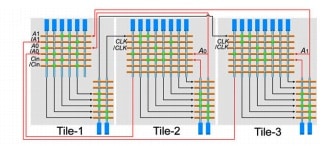
Three years ago we noted “the world’s first programmable nanoprocessor” achieved by a collaboration between Harvard and MITRE [also, see further details here]. This year the same interdisciplinary team has taken further key steps toward a functioning nanoelectronic computer based on integrating several of the tiles that they first reported three years ago. A hat tip to KurzweilAI for reprinting this news release from MITRE “MITRE-Harvard Team’s Ultra-tiny Nanocomputer May Point the Way to Further Miniaturization in Industry“:
An interdisciplinary team of scientists and engineers from The MITRE Corporation and Harvard University has taken key steps toward ultra-small electronic computer systems that push beyond the imminent end of Moore’s Law, which states that the device density and overall processing power for computers will double every two to three years. In a paper … in the Proceedings of the National Academy of Sciences [abstract; full text PDF courtesy of the Lieber Research Group], the team describes how they designed and assembled, from the bottom up, a functioning, ultra-tiny control computer that is the densest nanoelectronic system ever built.
The ultra-small, ultra-low-power control processor—termed a nanoelectronic finite-state machine or “nanoFSM”—is smaller than a human nerve cell. It is composed of hundreds of nanowire transistors, each of which is a switch about ten-thousand times thinner than a human hair. The nanowire transistors use very little power because they are “nonvolatile.” That is, the switches remember whether they are on or off, even when no power is supplied to them.
In the nanoFSM, these nanoswitches are assembled and organized into circuits on several “tiles.” Together, the tiles route small electronic signals around the computer, enabling it to perform calculations and process signals that could be used to control tiny systems, such as miniscule medical therapeutic devices, other tiny sensors and actuators, or even insect-sized robots.
In 2011, the MITRE-Harvard team demonstrated a single such tiny tile capable of performing simple logic operations. In their recent collaboration they combined several tiles on a single chip to produce a first-of-its-kind complex, programmable nanocomputer.
“It was a challenge to develop a system architecture and nanocircuit designs that would pack the control functions we wanted into such a very tiny system,” according to Shamik Das, chief architect of the nanocomputer, who is also principal engineer and group leader of MITRE’s Nanosystems Group. “Once we had those designs, though, our Harvard collaborators did a brilliant job innovating to be able to realize them.”
Construction of this nanocomputer was made possible by significant advances in processes that assemble with extreme precision dense arrays of the many nanodevices required. These advances also made it possible to manufacture multiple copies of the nanoFSM, using a groundbreaking approach in which, for the first time, complex nanosystems can be economically assembled from the bottom up in close conformity to a preexisting design. Until now, this could be done using the industry’s expensive, top-down lithographic manufacturing methods, but not with bottom-up assembly.
For this reason, the nanoFSM and the means by which it was made represent a step toward extending the very economically important five-decade-long trend in miniaturization according to Moore’s Law, which has powered the electronics industry. Because of limitations on its conventional lithographic fabrication methods and on conventional transistors, many industry experts have suggested that the Moore’s Law trend soon may come to an end. Some assert that this might occur in as little as five years and have negative economic consequences, unless there are innovations in both device and fabrication technologies, such as those demonstrated by the nanoFSM.
James Ellenbogen, chief scientist for nanotechnology at MITRE and an expert in the development of computers integrated on the nanometer scale, said, “The nanoFSM and the new methods that were invented to build it are not the whole answer for the industry. However, I believe that they do incorporate important steps forward in two of the key areas the electronics industry has been focused upon in order to extend Moore’s Law.”
In addition to Das and Ellenbogen, the development team at MITRE included James Klemic, the corporation’s nanotechnology laboratory director. The researchers from MITRE—a pioneer in the nanotechnology field since 1992—collaborated with a three-person team at Harvard, led by Charles Lieber, a world-leading nanotechnology investigator.
In this work the three tiles integrate 180 programmable transistor nodes into both computing and memory elements, which were successfully reprogrammed to form a 2-bit full adder. It will be interesting to watch how far this promising approach can be scaled.
—James Lewis, PhD
