Summary
An overview of projects spearheaded by the Advanced Manufacturing Office of the US Department of Energy. These projects, involving Atomically Precise Manufacturing, are part of a larger vision for energy efficiency. The diverse portfolio of projects includes molecular assembler tips, molecular lego, diamondoid tools, copper/carbon hybrid materials, DNA origami, and Microelectromechanical systems.
Presenters

Tina Kaarsberg, Department of Energy
I started on the Hill as an APS Congressional Science Fellow for Senator Domenici working on the Climate Change negotiations, the Earth Summit and the Energy Policy Act of 1992. Later, on the House side, I worked for Science Chairman Boehlert for EPACT 2005. Since then I have worked at the U.S. Department of Energy in a variety of positions including Policy Analysis, Geothermal program team leader…
Presentation: AMO’s program in Atomically Precise Manufacturing and Nanocarbon Materials
- Presenting today is Tina Kaarsberg of the US Department of Energy, Office of Energy Efficiency and Renewable Energy. She is part of the Advanced Manufacturing Office (AMO) and speaks about Atomically Precise Manufacturing.
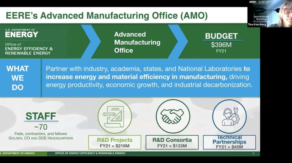
- AMO is involved in APM because it is a pathway toward energy efficiency. The Office of Energy Efficiency manages a budget of ~$400 million per year. More than half goes toward R&D of next generation materials process and energy supply technologies. Another ~$130 million goes toward R&D consortia such as Power America consortia for wide band semiconductors. The rest goes to technical partnerships.

- 6 guiding principles for AMO. In the past AMO has focused on reducing energy intensity of manufacturers and is still a primary focus. However, AMO now has a mandate to partner with manufacturers to make things that are more energy efficient. Most of Tina’s ideas going forward support the latter goal – expressed as reducing the life cycle energy and resource impacts of manufactured goods.
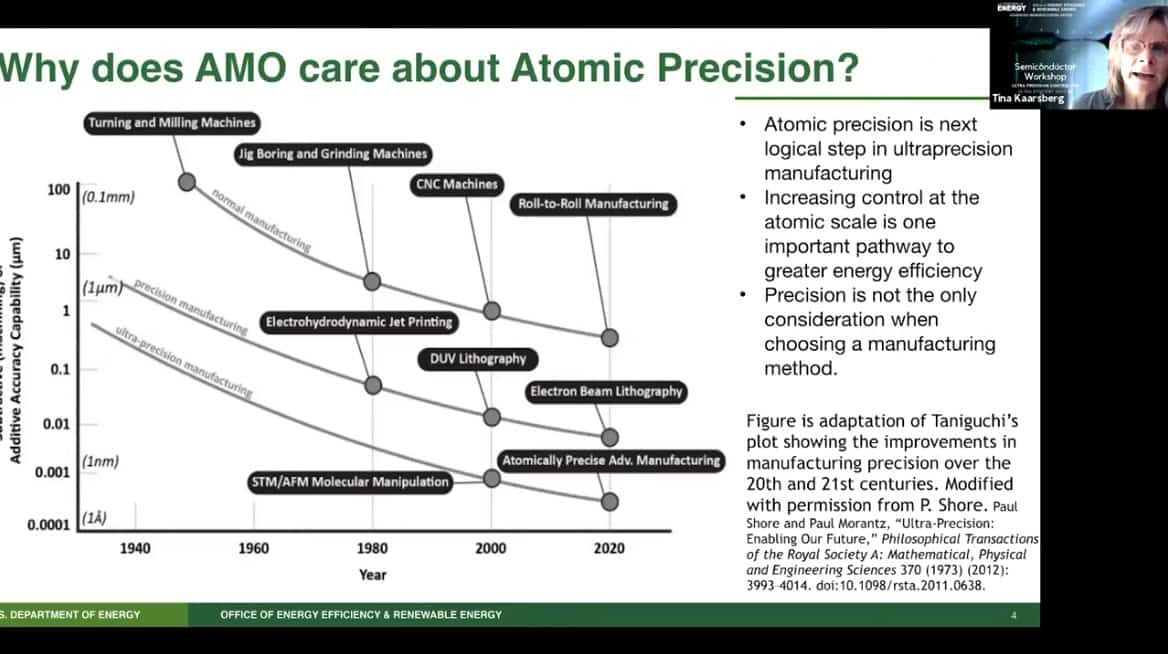
- The hypothesis driving us is that increasing control at the atomic scale is a pathway to greater energy efficiency. APM is the next step in a long history of ultra precise manufacturing techniques. AMO recognizes that much of the cutting edge is at the nano or even atomic scale. Semiconductor manufacturing is one of many field that will benefit from APM, and is likely the closest to commercialization.
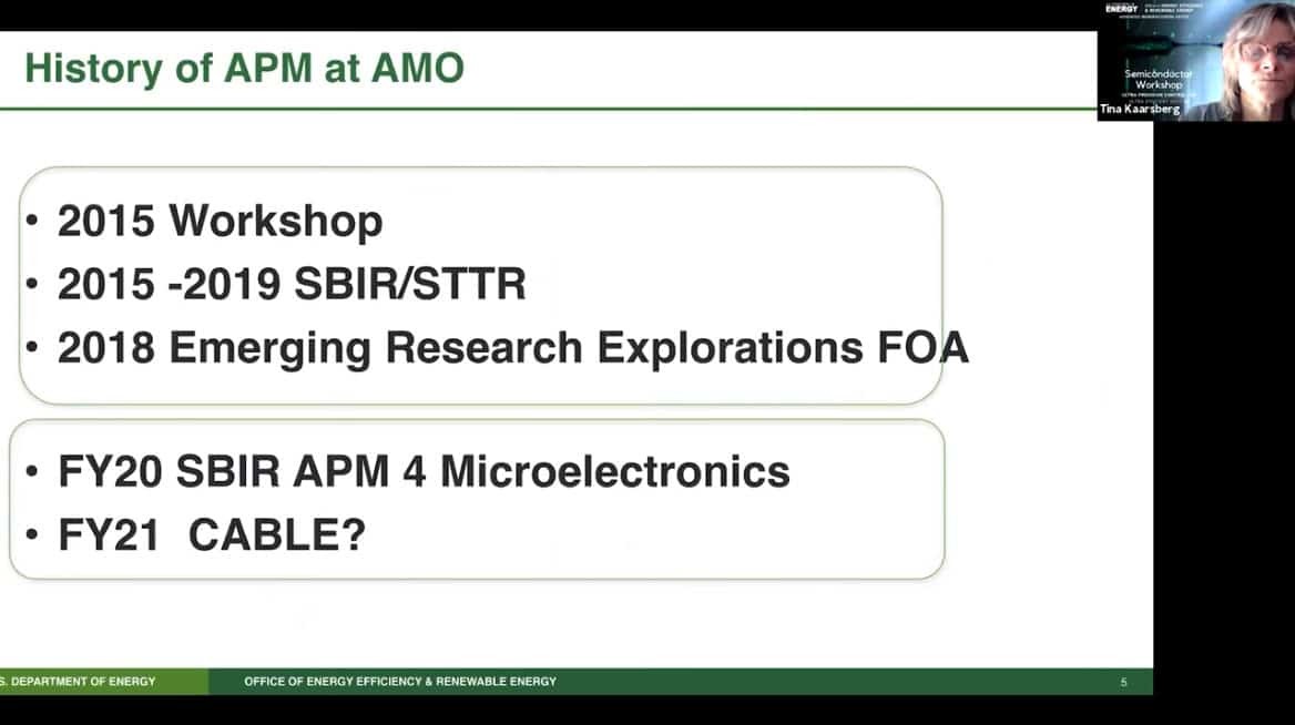
- Historical outline of the talk.
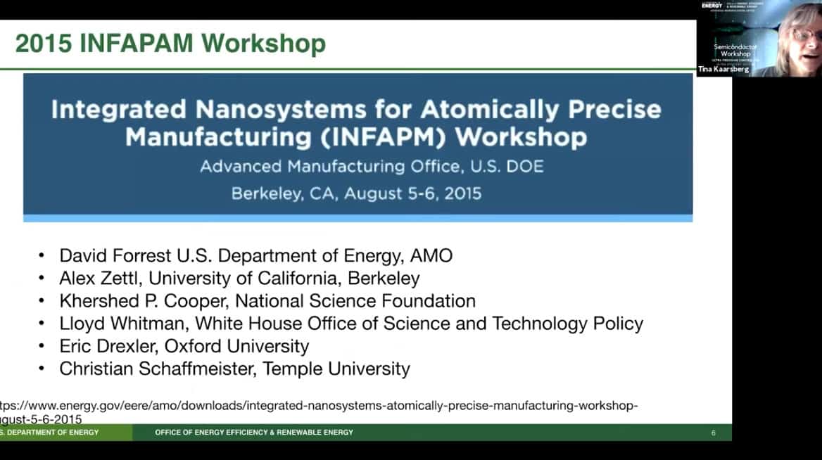
- Workshop on APM which was seminal in the development of the program.
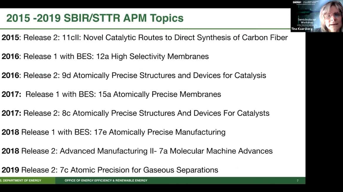
- The variations on SBIR topics tracks the evolution of AMO priorities. Many different projects were initiated over the years. One successful project was to create nanomembranes for oxygen generation. Another successful project involving catalysis discovered a detergent molecule. In 2018, STM lithography research was funded which has become the foundation of ultra energy efficient semiconductor device work. Nano-aluminum was also funded during this time and may become part of the APM portfolio.

- APM funding peaked in 2018 when $10.5 million of SBIR funding was matched with $8 million in Emerging Research Exploration funds.
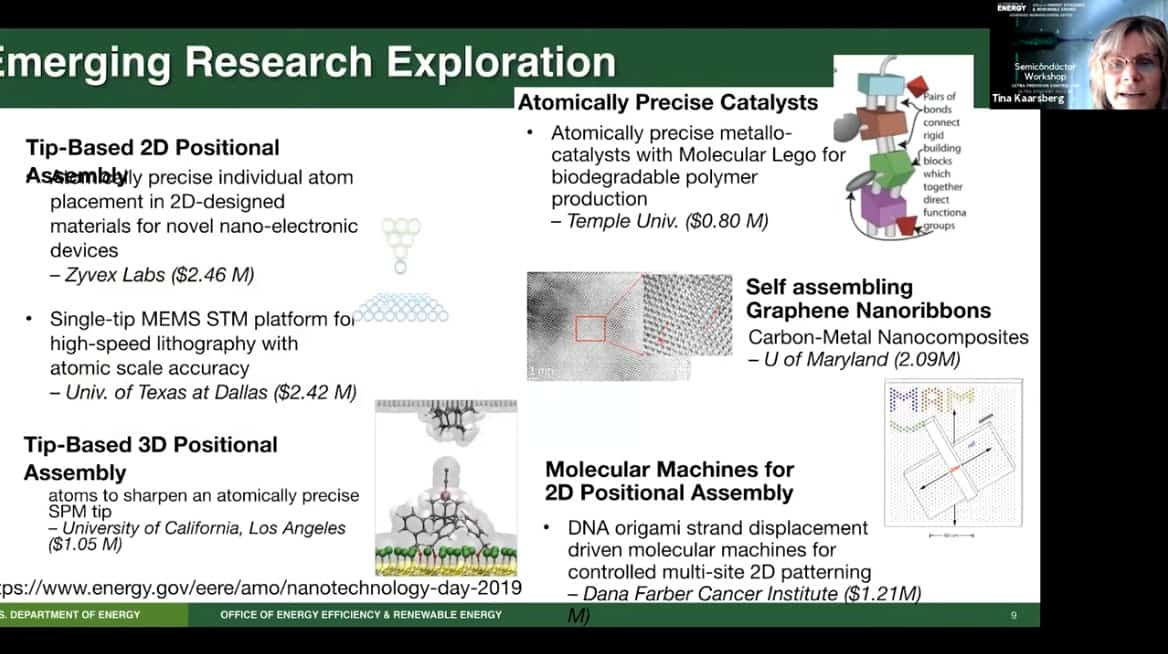
- Projects include 2d and 3d positional assembly, self assembling graphene nanoribbons, and atomically precise catalysts.
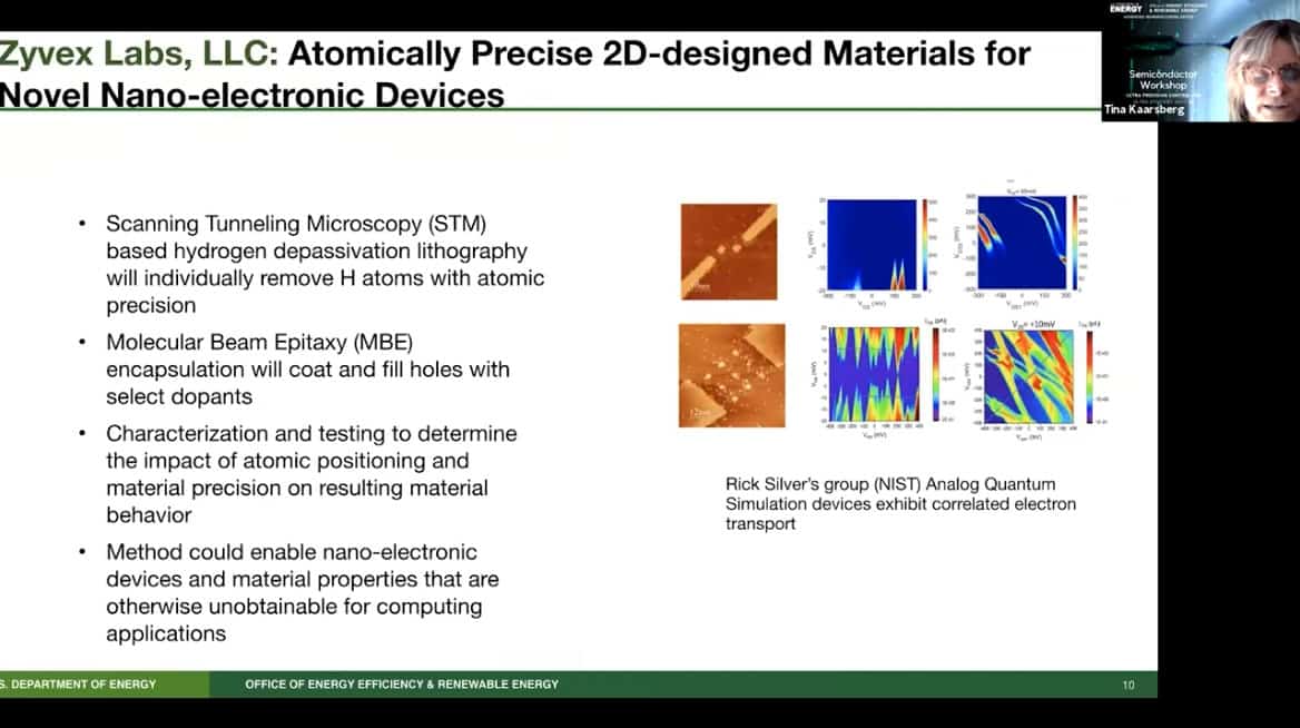
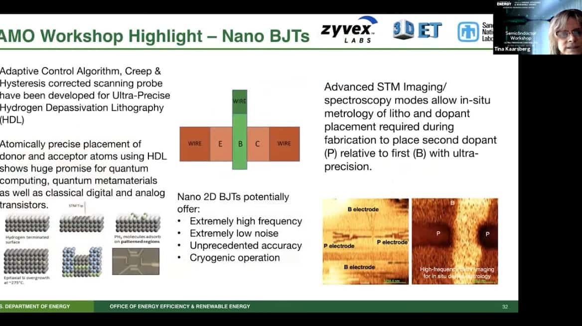
- One of the Zyvex projects involved using a scanning tunneling microscope to create atomically precise 2d materials. Individual hydrogen atoms were pulled out of a surface and substituted with others. This project had applications for quantum computing and nanoelectronic devices.
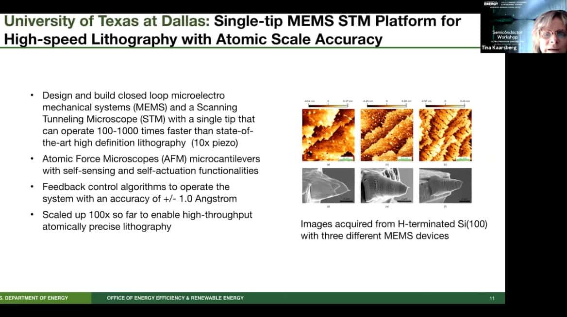
- University of Texas is working to increase the operating speed of molecular assembler microscope tips by a factor of 100 to 1000x via microfabrication technologies. You can see the different tips used and the different MEMS techniques used.

- The UCLA team was delayed when their partner was acquired by a Canadian banknote company. This technology of depositing atoms can be used to help prevent bank note fraud, but a more likely explanation is that the company has become the core of Canada’s $200 million atomically precise manufacturing program. Not much information has been released. The UCLA team is developing atomically precise tips by using a diamonoid tool to grab and position molecules to build atomically precise structures.
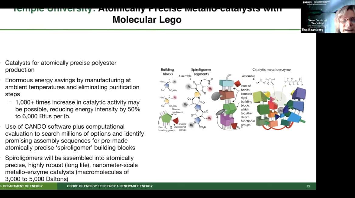
- Temple University has been designing and synthesizing atomically precise structures using unique molecular building blocks – molecular lego – to create energy efficient catalysts for polyester production. It could also increase the recyclability of polyester to reduce the environmental hazard from plastic buildup. Of the group, this is probably the most advanced manufacturing technology.
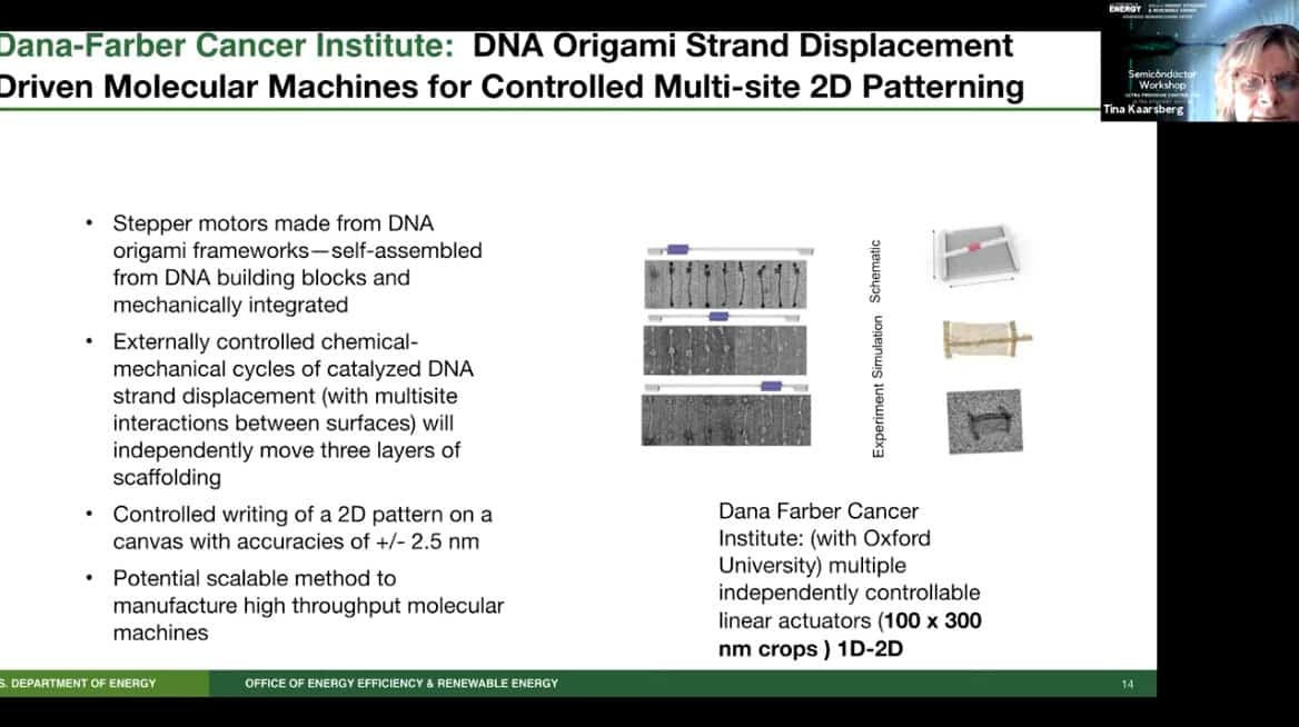
- The Dana-Farber cancer institute team is building a first of its kind molecular 2d printer that is itself atomically precise. It allows the creation of a picomole (10^12) of product simultaneously. This project was delayed severely by covid restrictions.
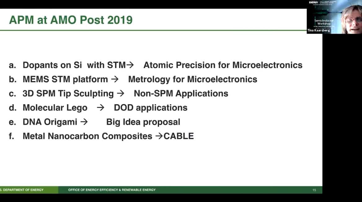
- An overview of the various projects:
- Dopants on silicon with STM → Atomic precision for microelectronics
- MEMS STM platform → Metrology for microelectronics
- 3D SPM Tip Sculpting → Non-SPM applications
- Molecular Lego → DOD Applications
- DNA Origami → Big Idea Proposal
- Metal Nanocarbon Composites → CABLE
- These projects were all delayed by covid but are getting back on track to meeting their goals.
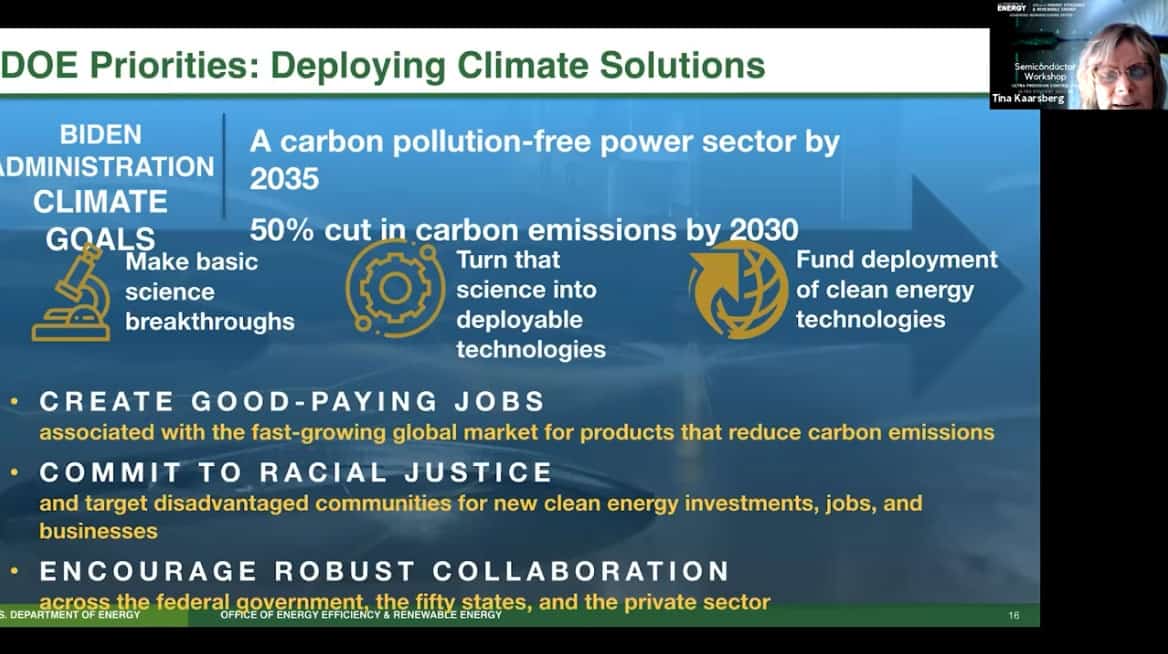
- The mission is to reach a zero carbon emission grid by 2035, and to reduce carbon emissions by 50% by 2030. There is also a need to bring semiconductor manufacturing back to the US.
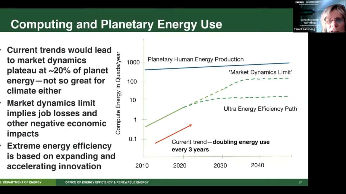
- Even without the need to reduce our impact on the climate, we need energy efficiency due to the rapid increase of energy use for manufacturing and the limit of how much energy can be produced worldwide.
- Atomic precision for microelectronics portfolio of projects.
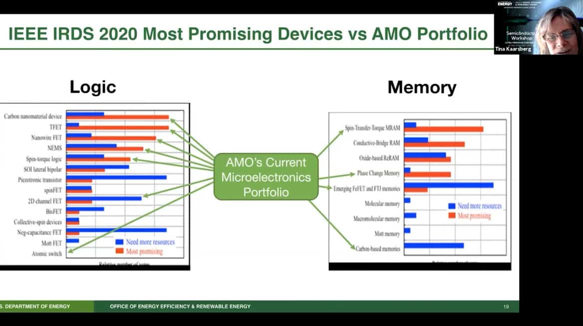
- We put out an SBIR asking for atomic precision for energy efficiency. It turns out the microelectronics portfolio that we got underpins the promising device types of the IEEE international roadmap on devices and systems.
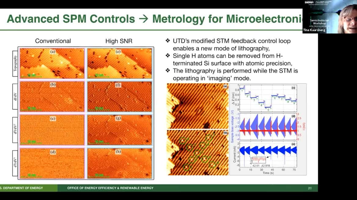
- Metrology – the scientific study of measurement – can also be greatly improved by atomic precision. The signal to noise ratio for STM signals was improved by MEMS imaging. It is possible to image individual atoms and at the same time remove them while STM is operating in imaging mode. 4 patents were awarded with 2 more pending for this technology.
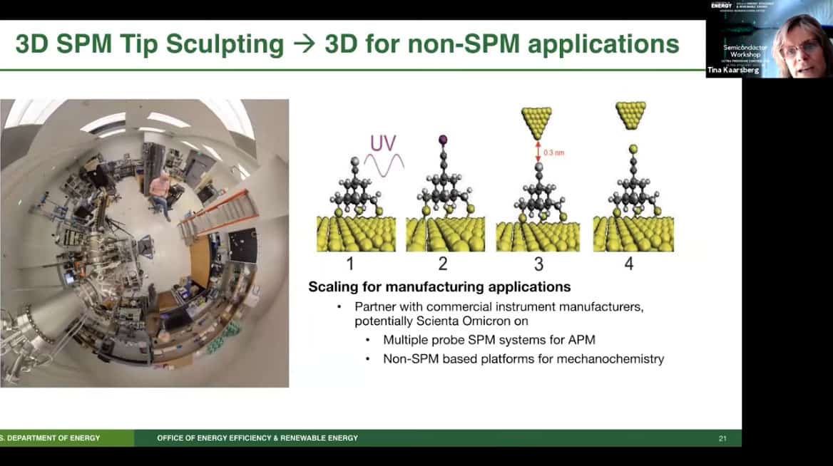
- The UCLA team, despite numerous delays, have created a diamondoid tool to extract single atoms. This project will benefit greatly from the speedup of atomic force microscope tips due to MEMS advances. Another thing about this project is that it took a lot of chemistry experimentation and modeling, and I confess I have the least background on this project.
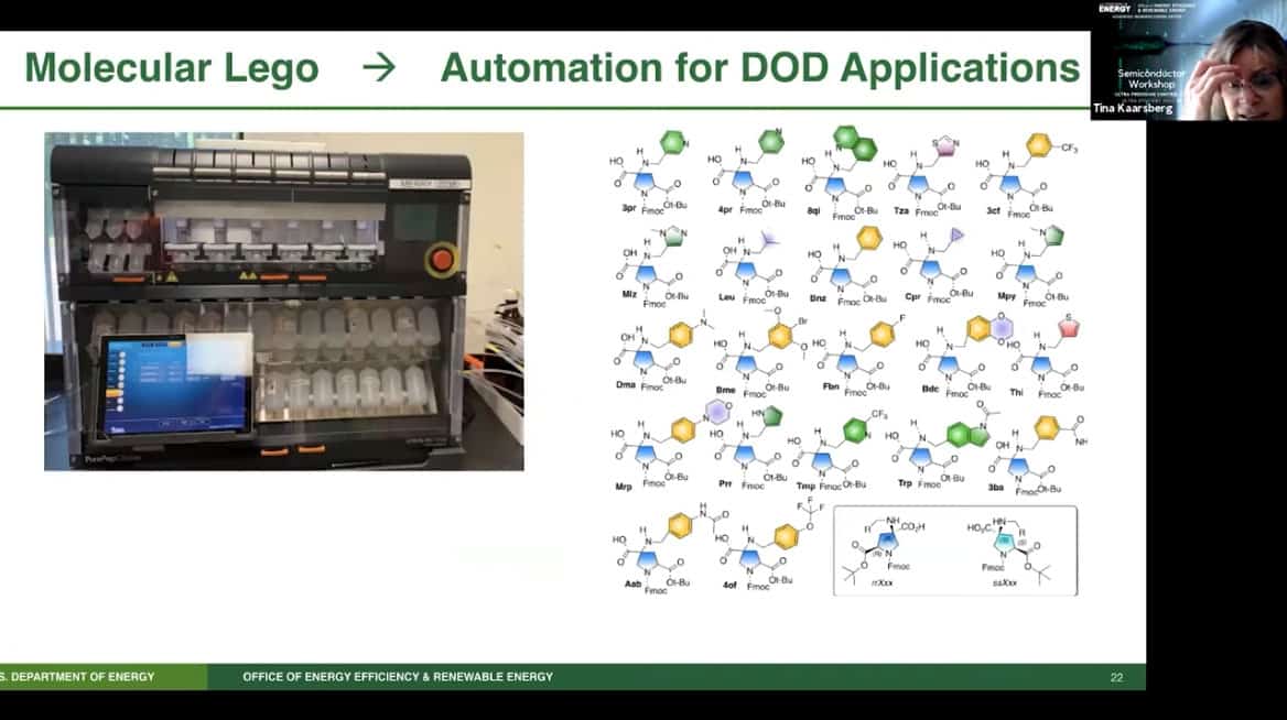
- Molecular lego is proceeding – the Department of Defense authorized them to acquire automated synthesis and purification equipment. The project throughput has increased by two orders of magnitude. They are on their way to creating selective polyester-forming macromolecular catalysts.

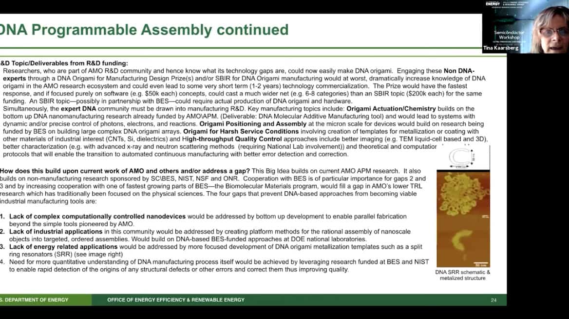
- My management has the hardest time understanding why this project should be part of AMO. I think this is exciting as a next gen manufacturing technology – because its using quaternary logic of DNA binding instead of binary. Stay tuned for my DNA origami PI William Shih to talk next month. I’m trying to figure out how an AMO effort in this area can support the 6 core goals. The US has an undisputed lead in biotech and it would be great to utilize that expertise to help with atomically precise manufacturing and energy efficiency.
- Another goal is to leverage domestic energy resources and materials, maybe enable rapid prototyping and recyclability design. We need to think about how to use electrical or chemical control rather than huge amounts of process energy.
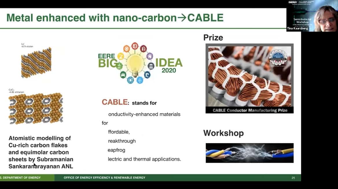
- Metal nanocarbon may be the project where AMO can really show its leadership on atomically precise manufacturing. CABLE stands for Conductivity-enhanced materials for Affordable Breakthrough Leapfrog Electric and thermal applications. This project involves assembling copper and carbon into specific patterns to create better power cables. It became apparent that we should also investigate metal enhanced without nanocarbon, either through rare earths or processing. There’s also the possibility of enhancing nonmetals with metal particles, such as using silver nanoparticles in a polymer.
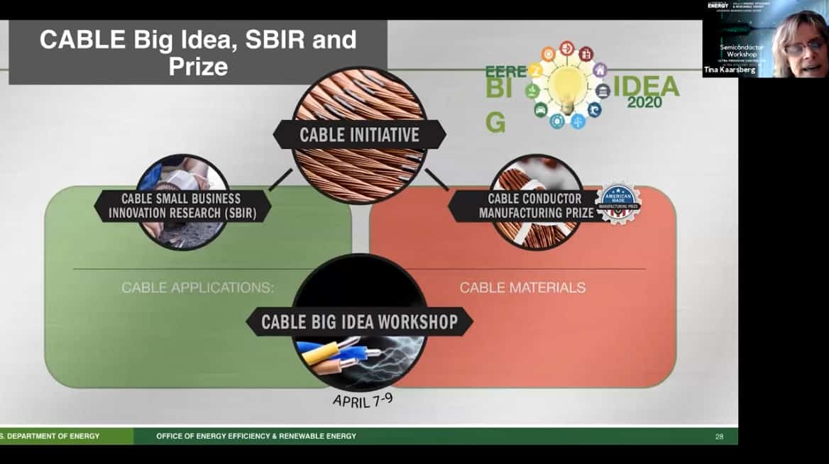
- Of the three stages of CABLE, only stage 1 is really cast. Stage 2 and 3 can be modified.

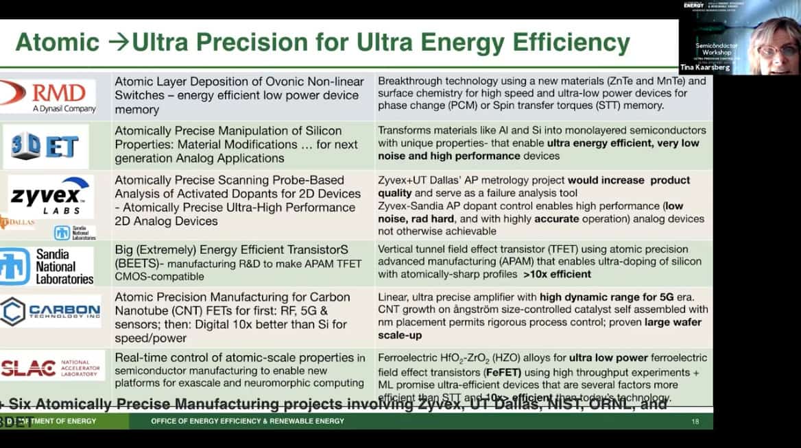
- This describes the vertical tunnel field effect transistor made with atomically precise manufacturing. They use molecular beam epitaxy and chemical vapor deposition to create these ultra-energy efficient transistors.
- This is describing a bipolar junction transistor

- Next is a dopant metrology project which is able to image phosphorous and boron dopants during fabrication.
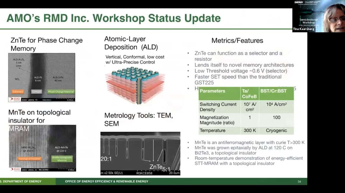
- RMD has an atomic-layer deposition project which uses interesting chemistry both for phase change memories and spin transfer torque device memory.
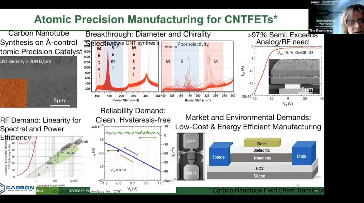
- A company called Carbon Technology is doing precision manufacturing of carbon nanotube field effect transistors, purifying carbon nanotubes to 95% metallic.
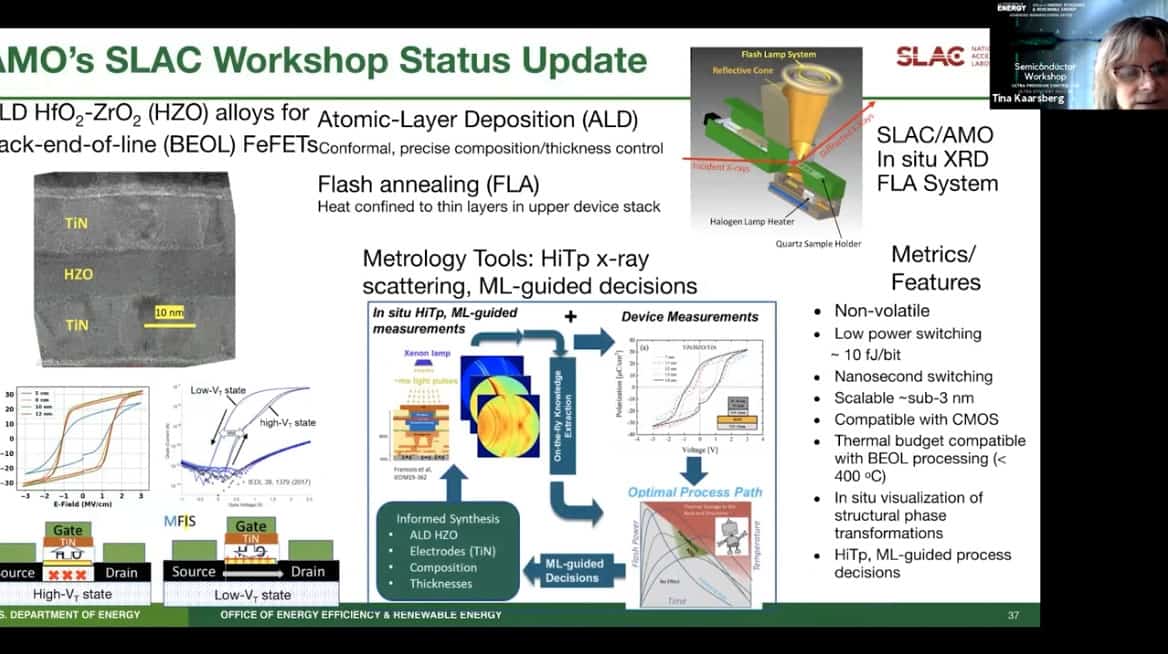
- SLAC project uses atomic layer deposition and flash annealing to work on ferroelectric memory. The project is also using machine learning to figure out how to design and optimize the process.
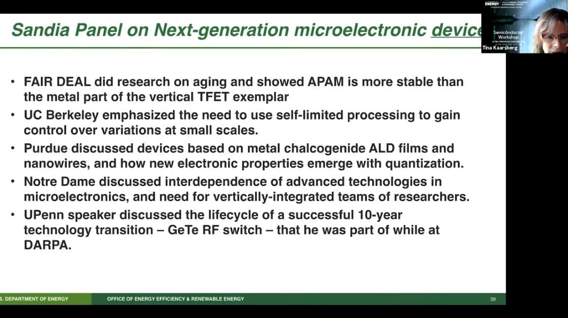
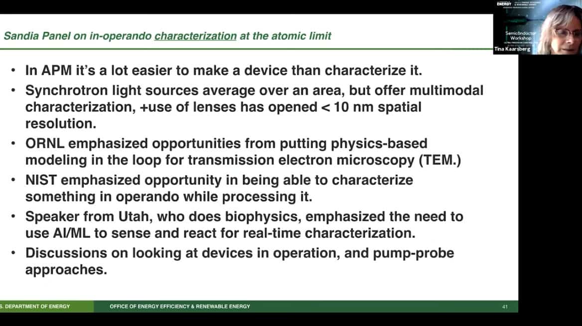
- There was a relevant workshop on atomic precision on April 20-21, 2021. From my notes on the workshop – one of the great results was showing atomically precise results from a TFET showing APAM is more stable than the metal part. The workshop talked about various forms of fabrication. Also the difficulty of characterization.
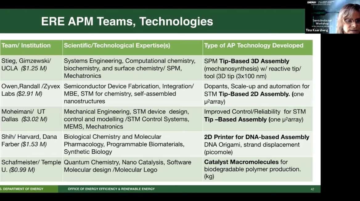
- An overview of APM teams
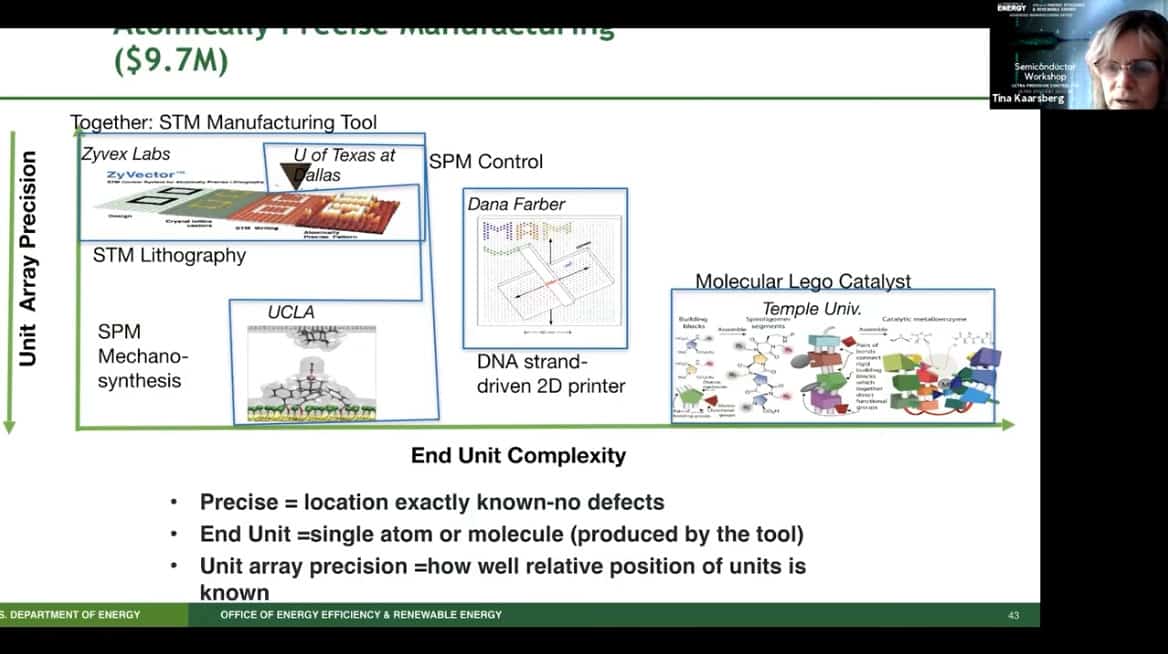
- An overview of end unit complexity
Q&A
Regarding the goal of semiconductor energy efficiency – what about E3S Center at Berkeley?
- We are aware of their organization but they are no longer funding projects.
Atomic precision – its one thing to create a few dozen atoms on a surface and another to scale it up. Do any of the programs attempt to bridge the gap to scale up to much larger sizes?
- For STM manufacturing, ultradoping leads to interesting phenomena such as abrupt dopant profile – important for the tunnel field transistor. The tunnel field transistor is projected to be about 10x more efficient, which is the type of advance we need to get to these ambitious goals. Area select deposition is being investigated (guided self assembly) for scale-up of ultradoped devices. They’ve done some testing and it looks like ASD can be used to manufacture these vertical tunnel field transistors.
Can ultra low K dielectric materials be of interest?
- Yes, we talked about ultra low K dielectric materials and how it was one of the ways that we can deal with the end of Moore’s law in certain applications.
Is there plenty of room in the middle?
- Yes, that was a major result at the workshop last week. We want to do as much bottom up as possible, because the top down aspect requires fighting entropy so much. However, using the top down approach gives us an understanding of technologies which can be useful in other applications as well.
Is CABLE what used to be called Covetics?
- Yeah, Covetics was the research program I took over and it’s what led to the idea of the CABLE initiative.
Given that there are lots of researchers in the group seeking to make their discoveries applicable, what areas should attention be drawn to?
- Carbon reduction is generally a really important area.
- DNA origami should get more supporters.
Molecular precision for carbon capture seems like a good idea?
- The Office of Fossil Energy usually talks about carbon capture – their view is typically an end of pipe view whereas our view is to prevent its creation in the first place.
How can we track your research and projects?
- Nanotechnology day is a good excuse to package work together to share with the public. Search for it on google and you will find links to a lot of past and future projects being worked on by AMO.
- https://www.energy.gov/eere/amo/nanotechnology-day-2020
What workshops could be useful for this group?
- [need urls here] CABLE-big-idea
- Semiconductor workshop series
- Virtual workshops
Seminar summary by Aaron King.