Electrical characterization of nanowires created by metallization of a
biological template
Wolfgang Fritzsche*, a, Remo
Kirschb, Konrad J. Böhmc, Eberhard
Ungerc, Thomas Wagnerd, Michael Mertigb,
J. Michael Köhlera
a
Institute of Physical High Technology Jena
bTechnical University Dresden
cInstitute of Molecular Biotechnology Jena
dFriedrich-Schiller-University Jena
This is an abstract
for a presentation given at the
Sixth
Foresight Conference on Molecular Nanotechnology.
The full article is available at http://www.foresight.org/Conferences/MNT6/Papers/Fritzsche/index.html.
Molecular electronics emerges as a possibility to continue the miniaturization of electronic circuits down to the lower nanometer scale. One significant challenge is the electrical connection of molecular devices by nanowires.
We present here the use of metallized microtubules as such a molecular wire. Microtubules (tube-like protein structures of 24 nm diameter; Vater et al., 1995) were metallized (Kirsch et al., 1997) and deposited on microstructured substrates (Fig. 1). Electron beam-induced deposition (EBD) was used for structuring of connecting gold lines, which wire a single microtubule to microelectrodes created by photolithography (Fig. 2) (Fritzsche et al., 1998).
The electrical characterization yielded an Ohmic behavior for the
metallized protein structure with a resistance of about 1 kOhm over a
length of several microns (Fig. 3). This bio-templating approach was
extended to other biomolecules (e.g., DNA); and electrical measurements on
DNA-based nanowires will be presented.
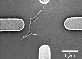
Fig. 1: Metallized microtubules deposited on a
prestructured substrate
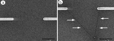
Fig. 2: A thin gold coating is applied to the microtubules prior to structuring of contacts by means of electron beam deposition (EBD). Bar = 5 micrometer. a) Gold-coated substrate. b) Substrate after writing of EBD-lines (arrows), which mask the gold in a subsequent dry-etching step.
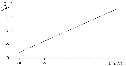
Fig. 3: Electrical mesurement on a metallized microtubule.
References:
- Fritzsche, W., Böhm, K. J., Unger, E. and Köhler, J. M. (1998). Nanotechnology (in press). Making electrical contact to single molecules
- Kirsch, R., Mertig, M., Pompe, W., Wahl, R., Sadowske, G. and Unger,
E. (1997). Thin solid films, 305, 248-253. Three-dimensional metallization
of microtubules
- Vater, W., Fritzsche, W., Schaper, A., Böhm, K. J., Unger, E. and
Jovin, T. M. (1995). J. CellSci., 108, 1063-1069. Scanning force microscopy
of microtubules and polymorphic tubulin assemblies in air and in liquid
*Corresponding Address:
Wolfgang Fritzsche
Institute of Physical High Technology
PO Box 100 239, D-07702 Jena, Germany
phone: xx49-3641-657744, fax: -657700,
email: [email protected],
homepage
|