
Atomic-level sculpting of a crystalline oxide from a metastable amorphous oxide film has been demonstrated using a scanning transmission electron microscope. A hat tip to KurzweilAI for reporting this Oak Ridge National Laboratory news release “New electron microscopy method sculpts 3-D structures at atomic level“:
Electron microscopy researchers at the Department of Energy’s Oak Ridge National Laboratory have developed a unique way to build 3-D structures with finely controlled shapes as small as one to two billionths of a meter.
The ORNL study published in the journal Small demonstrates how scanning transmission electron microscopes, normally used as imaging tools, are also capable of precision sculpting of nanometer-sized 3-D features in complex oxide materials.
By offering single atomic plane precision, the technique could find uses in fabricating structures for functional nanoscale devices such as microchips. The structures grow epitaxially, or in perfect crystalline alignment, which ensures that the same electrical and mechanical properties extend throughout the whole material.
“We can make smaller things with more precise shapes,” said ORNL’s Albina Borisevich, who led the study. “The process is also epitaxial, which gives us much more pronounced control over properties than we could accomplish with other approaches.”
ORNL scientists happened upon the method as they were imaging an imperfectly prepared strontium titanate thin film. The sample, consisting of a crystalline substrate covered by an amorphous layer of the same material, transformed as the electron beam passed through it. A team from ORNL’s Institute for Functional Imaging of Materials, which unites scientists from different disciplines, worked together to understand and exploit the discovery.
“When we exposed the amorphous layer to an electron beam, we seemed to nudge it toward adopting its preferred crystalline state,” Borisevich said. “It does that exactly where the electron beam is.”
The use of a scanning transmission electron microscope, which passes an electron beam through a bulk material, sets the approach apart from lithography techniques that only pattern or manipulate a material’s surface.
“We’re using fine control of the beam to build something inside the solid itself,” said ORNL’s Stephen Jesse. “We’re making transformations that are buried deep within the structure. It would be like tunneling inside a mountain to build a house.”
The technique offers a shortcut to researchers interested in studying how materials’ characteristics change with thickness. Instead of imaging multiple samples of varying widths, scientists could use the microscopy method to add layers to the sample and simultaneously observe what happens.
“The whole premise of nanoscience is that sometimes when you shrink a material it exhibits properties that are very different than the bulk material,” Borisevich said. “Here we can control that. If we know there is a certain dependence on size, we can determine exactly where we want to be on that curve and go there.”
Theoretical calculations on ORNL’s Titan supercomputer helped the researchers understand the process’s underlying mechanisms. The simulations showed that the observed behavior, known as a knock-on process, is consistent with the electron beam transferring energy to individual atoms in the material rather than heating an area of the material.
“With the electron beam, we are injecting energy into the system and nudging where it would otherwise go by itself, given enough time,” Borisevich said. “Thermodynamically it wants to be crystalline, but this process takes a long time at room temperature.”
The study is published as “Atomic-level sculpting of crystalline oxides: towards bulk nanofabrication with single atomic plane precision” (abstract).
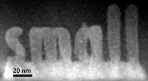
Atomically precise fabrication of complex 3-D objects has been demonstrated—for certain nanostructures composed of certain materials under certain conditions. Atomic-level sculpting was accomplished using scanning transmission electron microscopy (STEM) in high-angle annular dark-field imaging (HAADF) and electron-beam sculpting. Sculpting was implemented by using the electron beam to convert a thin film of amorphous strontium titanate, covering a crystalline strontium titanate substrate, into the crystalline material, followed by removal of the remaining amorphous material. The electron beams used for sculpting were 100 to 200 keV. The crystallization rate and epitaxial growth rate were controlled by controlling electron dose and dose rate. The atomically focused electron beam induced solid phase epitaxial growth, allowing, with improved methods of beam path control, sculpting of crystalline features as small as 1-2 nm. The research paper shows the letters “ORNL” patterned on a previously amorphous region of SrTiO3 in letters 20 nm high. Since the lattice spacing of the epitaxial structure is reported as 0.39 nm, inspection of the hi-res portions of the image suggests that the precision of the sculpting is indeed close to atomically precise. The authors propose “We believe this technique can be further developed into a nanoscale complementary approach to 3D printing.”
How close does this “atomic-level sculpting” come to atomically precise manufacturing? It will be interesting to see how far the method evolves toward fabricating arbitrarily large and complex structures, but a few obvious limitations include:
- Nanofabrication is limited to nanostructures composed of one crystalline structure.
- Like the metal oxide used here, the substance chosen must have a metastable amorphous phase that can be nudged by an electron beam into a unique crystalline state.
- Error rates in epitaxial growth and precision in guiding the electron beam may limit the size and complexity of the structures that can be fabricated.
- Could this method be adapted to mechanical systems with moving parts?
Different methods of achieving, or at least approaching, atomic precision for different purposes are being reported. This top-down method joins recent bottom-up examples like synthetic molecular motors and DNA nanomachines. These methods are likely to undergo continued improvement, and perhaps be used in important near- and mid-term applications. Which, if any, will ultimately lead to general purpose high-throughput atomically precise manufacturing remains to be seen.
—James Lewis, PhD