A select set of videos from the 2013 Foresight Technical Conference: Illuminating Atomic Precision, held January 11-13, 2013 in Palo Alto, have been made available on vimeo. Videos have been posted of those presentations for which the speakers have consented. Other presentations contained confidential information and will not be posted.
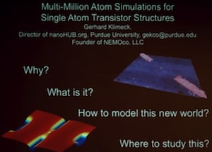
The 8th speaker at the Atomic Scale Devices session was Gerhard Klimeck. His talk was titled “Multi-Million Atom Simulations for Single Atom Transistor Structures” biography and abstracts, video – video length 26:37.
From an electrical engineer’s perspective, Prof. Klimeck began with the observation that over the years the number of transistors on a chip has increased exponentially to more than two billion transistors on a chip, but for the last six to eight year the clock speed has not increased beyond two gigahertz because the power consumption on the chip, about 100 watts per square centimeter, limits the clock speed. Currently the major contribution to this power consumption is “static power”—the power leaking through the transistor whether it is switching or not. The amount of leakage is a fundamental limit of the thermal distribution of charge carriers in the CMOS chip. A solution would be to develop a tunneling transistor that is no longer thermally limited, but instead gives current flow in a narrow energy window. Modeling potential solutions, such as a double gate or a nanowire, to see how current flow can be modulated by the gate of transistor requires an atomistic modeling tool. We and others have shown that nanowire gates can dramatically reduce voltage, so that tunneling transistors may be able to solve the power consumption problem, but perhaps only for a short time. One multi-gate device called a finFET depends on a thin silicon “fin”, so that although the device is nominally a 22-nm device, the active region is only 8 nm wide—64 atoms. In devices currently of interest the number of critical atoms can be as low as 14. This is the reason Klimeck’s group has been building their NEMO (NanoElectronicMOdeling) tool. Further, the number of electrons under the gate in today’s technology is already in the hundreds and is rapidly approaching the tens. So the regime of single electron and quantum dot devices is not so far away. Thus Klimeck’s NEMO tool spans the range from modeling current devices to designing single electron and quantum dot devices.
Klimeck presented examples where they have seen single electron effects in finFETs. They are able to fingerprint the devices and with modeling identify impurities due to the presence of arsenic atoms instead of phosphorous atoms.Another device called a coulomb diamond allows identification of the number of electrons sitting in the device. Modeling a device built by Michelle Simmons of the University of New South Wales, Australia, they were able to show that the device was a single atom transistor, but in this case, it was not an erroneous atom in a finFET, but rather a single atom that Michelle had deliberately placed. Have been working with Michelle Simmons to understand the electronic structures of these device components: 2D sheets, nanowires, single atom impurities. They were able to show, for example, that Ohm’s Law held for a nanowire four atoms wide and one atom tall [“Ohm’s Law Survives to the
Atomic Scale” B. Weber et al. Science 335: 64-67 (212)]. The NEMO tool has been validated against other theories, but what these theories cannot do is increase the size of the domain modeled and look at disorder. Likewise, the potential can be calculated for single electron devices by looking at the potential over a large domain. The NEMO tool has been developed over 18 years and multiple generations of code to model the devices one atom at a time. Currently the group working on NEMO 5 includes 6 professionals and 21 students working on the code. It scales to the peta scale and can run on 220,000 cores, so that running for one hour is like running for 25 years on a single CPU. These programs are available on nanoHUB, the largest user facility in the world, with 250,000 users.
Prof. Klimeck briefly described the methodology used for NEMO as representing atoms by tight binding so that they could look at valence electrons in general. They can include strain and deformations of the crystal, etc. to get eigenstates. Non-equilibrium Green’s functions are used to treat quantum transport including nuclear interactions, etc. A rate equation approach is used for coulomb blockade-type things. The key element is doing an electrostatic calculation over a huge domain that considers all the charges and all the effects of gates around it.
—James Lewis, PhD


