 A select set of videos from the 2013 Foresight Technical Conference: Illuminating Atomic Precision, held January 11-13, 2013 in Palo Alto, have been made available on vimeo. Videos have been posted of those presentations for which the speakers have consented. Other presentations contained confidential information and will not be posted.
In his introductory comments, Conference Co-Chair Larry S. Millstein stressed that the five sessions of the Conference were designed to bring together five research communities that have until now not had close contacts, in the hope that their interactions would accelerate progress. Similarly, the Conference’s restrictive media policy was designed to accelerate progress by encouraging speakers to share with Conference participants unpublished research by assuring them that sharing these results would not interfere with their future publication. http://vimeo.com/62028032 video length 3:49.
In his introductory comments, Conference Co-Chair J. Fraser Stoddart observed that for a quarter of a century nanotechnology has been bringing together physicists, chemists, biologists, material scientists, engineers, and computational people under the banner of “nano”. He referred to his own recent work as an example of the self-assembly of simple structures to produce emergent complex behavior, and expressed the desire that this assembly bringing together widely divergent scientific, technological and engineering perspectives would inspire new knowledge. http://vimeo.com/62028033 video length 7:36.
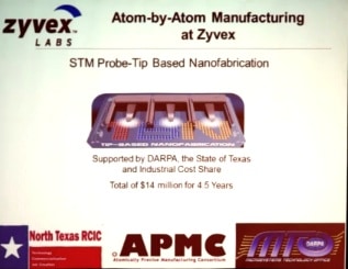
John Randall introduced the session on Atomic Scale Devices and discussed work at Zyvex Labs on “Atomically Precise Manufacturing”. http://vimeo.com/62119582 – video length 28:52. Randall made clear at the onset that by atomic precision, he is not talking about a precision of plus or minus one atom, but rather about absolute precision in manufacturing—no size variation. You put the atoms where you want them so everything is the same and matter can be dealt with as though it is digital. There is no accumulation of error and eventually materials can be defect free. He proposed that once absolute precision is achieved that the volume of material that could be produced cost effectively would increase exponentially, making an “educated guess” that using techniques that they are working on today, they will reach one cubic micrometer before 2020. He described the Atomically Precise Manufacturing Consortium and their commitment to bring atom-by-atom manufacturing tools to market. Their approach uses an STM to precisely remove individual hydrogen atoms from the surface of a passivated crystal, followed by atomic layer epitaxy to build three-dimensional structures with top-down control, “putting every atom where we want it.” Randall emphasized that the STM tip is not used to drag Si or H atoms around and into place; it is only used to image and for electron-stimulated desorption of passivated hydrogen atoms. Examples of products that might start this proposed exponential manufacturing trend include a nanometrology standard consisting of a wall of silicon a know number of atoms wide and a known number of atoms tall, NEMS resonators that operate in the terahertz regime, master templates for nanoimprinting, devices for quantum computing, and nanopores for ultra-high-speed DNA sequencing.
—James Lewis, PhD