Three years ago Australian and American physicists created a working transistor from a single atom using a scanning tunneling microscope to precisely remove individual hydrogen atoms from the surface of a silicon crystal. Such technology provides a valuable laboratory demonstration of something close to the ultimate limits of computer technology, but a path from laboratory demonstration to economical fabrication of commercial quantities of circuit components remains a very challenging research goal. However, on a scale one or two orders of magnitude larger than atomic precision, but with the added advantage of building in three dimensions rather than being limited to a surface, physicists at IBM are developing “directed self-assembly” to use a certain type of polymer molecule to push current photolithography further into the low nanometer-scale realm. From a report in MIT Technology Review written by Katherine Bourzac “3-D Transistors Made with Molecular Self-Assembly“:
Researchers at IBM have made the first 3-D transistors using a promising new manufacturing approach
A new way of building computer chips is taking shape that involves synthesizing molecules so that they automatically assemble into complex structures—which then serve as templates for etching nanoscale circuitry into silicon. The approach could let the computer industry continue to shrink electronics beyond the resolution of existing manufacturing machinery. IBM researchers have been the first to make speedy 3-D transistors using this new method.
In 2011, the computer industry adopted 3-D transistors for high-end integrated circuits because they switch faster while consuming less power than planar ones (see “How Three Dimensional Transistors Went from Lab to Fab”). Such circuits have conventionally been made via photolithography, the same process used for most computer circuits. In this process, silicon wafers are coated with a light-sensitive material called a photoresist, and then are exposed to a pattern made by shining light through a filter known as a mask. Wherever light strikes, the photoresist cures; the rest is washed away, and the wafer is then etched chemically to create features in exposed parts of the surface.
For the fastest microchips, which have elements as small as 22 nanometers and 80 nanometers apart, this process is repeated about 30 times, says Kwok Ng, director of nanomanufacturing at the Semiconductor Research Corp. in North Carolina. Each step requires its own expensive mask, and every step adds time to the process. Photolithography will work for the next generation of chips, with features 14 nanometers in size. But for faster chips with smaller features, photolithography will become too expensive and complicated, and will run into limits determined by the wavelength of light.
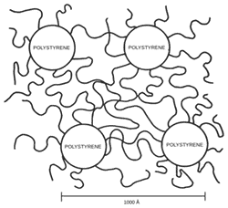
The IBM group used a new approach known as “directed self-assembly,” using a class of materials called block copolymers (polymer chains are made up of two kinds of monomers, or blocks). …
The article goes on to explain how the researchers adjusted various characteristics of the polymers to make smaller, denser parts than can be achieved using conventional lithography, thus reducing the distances between features from 80 nm to 29 nm. Some chipmakers are already testing directed self-assembly, the article reports, but whether or not it can be controlled well enough to be commercially successful remains to be seen.
—James Lewis, PhD
