
The path of progress in nanotechnology stretches from approximate control of the structure of matter—a precision of 1 to 100 nm in at least one dimension in which unique phenomena enable novel applications—to atomic precision in three dimensions. We at Foresight have been primarily interested in mechanical properties of systems of atomically precise machines. Progress along this path leads toward productive nanosystems and inexpensive high throughput atomically precise manufacturing. Current computer and other important technologies, however, rely upon electronic and optoelectronic properties. For these applications, progress toward atomically precise thin films, especially thin films of semiconductors, looks very promising. A hat tip to ScienceDaily for reprinting this Cornell University news article written by Anne Ju “Chemists cook up three atom-thick electronic sheets“:
Making thin films out of semiconducting materials is analogous to how ice grows on a windowpane: When the conditions are just right, the semiconductor grows in flat crystals that slowly fuse together, eventually forming a continuous film.
This process of film deposition is common for traditional semiconductors like silicon or gallium arsenide – the basis of modern electronics – but Cornell scientists are pushing the limits for how thin they can go. They have demonstrated a way to create a new kind of semiconductor thin film that retains its electrical properties even when it is just atoms thick.
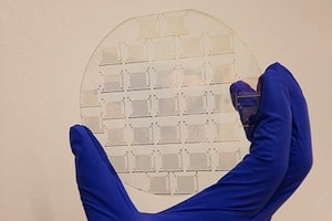
Three atom-thick layers of molybdenum disulfide were cooked up in the lab of Jiwoong Park, associate professor of chemistry and chemical biology and member of the Kavli Institute at Cornell for Nanoscale Science. The films were designed and grown by postdoctoral associate Kibum Kang and graduate student Saien Xie. Their work is published online in Nature, April 30 [abstract].
“The electrical performance of our materials was comparable to that of reported results from single crystals of molybdenum disulfide, but instead of a tiny crystal, here we have a 4-inch wafer,” Park said.
Molybdenum disulfide, which is garnering worldwide interest for its excellent electrical properties, has previously been grown only in disjointed, “archipelago”-like single crystal formations, Park said. But making smooth, flat, ultrathin sheets, like paper, is the ultimate goal, and the bridge to actual devices.
The researchers pulled off the feat by tuning the growth conditions of their films using a technique called metal organic chemical vapor deposition (MOCVD). Already used widely in industry, but with different materials, it starts with a powdery precursor, forms a gas and sprinkles single atoms onto a substrate, one layer at a time.
Park’s group systematically optimized the technique to make the films, tweaking conditions and temperatures not unlike experimenting in the kitchen. They found that their crystals grew perfectly stitched together, but only with a little bit of hydrogen and in completely dry conditions, for example. In addition to advanced optical imaging techniques, researchers led by co-author David Muller, professor of applied and engineering physics and director of Cornell’s Kavli Institute, contributed advanced transmission electron microscopy to test and characterize the quality of the films as they went along.
The team also demonstrated their films’ efficacy when stacked layer by layer alternating with silicon dioxide and employing standard photolithography. This effectively proved that these three-atom-thick semiconducting films can be made into multi-level electronic devices of unsurpassed thinness.
The MOCVD method for thin film generation is seemingly generic. The researchers showed the ability to simply change the precursor to make other films; for example, they also grew a tungsten disulfide film with different electrical properties and color. They envision perfecting the process to make atomically thin films of all varieties, like a packet of colored paper, from which new, exciting electronic and optoelectronic devices can be derived.
“These were only the first two materials, but we want to make a whole palette of materials,” Park said.
A PDF with the full text of the paper can be downloaded from the Park Group’s Publications page. A key finding is that layer-by-layer growth only occurs at low partial pressure of molybdenum vapor, produced by thermal decomposition of Mo(CO)6 in the presence of excess (C2H5)2S. Growth at higher pressures of Mo vapor produced a mixture of monolayer, multilayer, and no-growth regions on the 4-inch wafer. Also, getting large grains (about 1 µm) sizes and proper stitching of the grains together to form a continuous polycrystalline monolayer required introducing the proper amount of molecular hydrogen and eliminating moisture. Further, the electrical properties of devices (field effect transistors) fabricated at random locations in the monolayer showed nearly identical characteristics, indicating grain boundaries with low levels of defects. The authors state they have been able to use this method to grow transition-metal dichalcogenides on a variety of substrates in addition to SiO2.
… Our versatile MOCVD growth therefore
provides a new avenue for the growth, patterning and integration
of multiple high-quality monolayer TMD films with different compositions
and electrical properties on a single substrate, enabling the
future development of atomically thin integrated circuitry.
If their expectations are realized, this work could be a huge step toward atomically precise thin layers specifically, and more generally a major step toward atomically precise fabrication of electronic and optoelectronic devices.
—James Lewis, PhD