
We have been following progress toward using graphene nanoribbons in nanotechnology for nearly a decade, most recently citing “Atomically precise boron doping of graphene nanoribbons“. Just published results from Joseph W. Lyding, winner of the 2014 Foresight Institute Feynman Prize, Experimental category, and his collaborators have demonstrated a major step toward integrating atomically precise graphene nanoribbons onto a semiconductor surface. A hat tip to first author Adrian Radocea for sending word of their accomplishment described in this Beckman Institute news release written by Maeve Reilly “Creating Atomic Scale Nanoribbons“:
Silicon crystals are the semiconductors most commonly used to make transistors, which are critical electronic components used to carry out logic operations in computing. However, as faster and more powerful processors are created, silicon has reached a performance limit: the faster it conducts electricity, the hotter it gets, leading to overheating.
Graphene, made of a single-atom-thick sheet of carbon, stays much cooler and can conduct much faster, but it must be [fabricated] into smaller pieces, called nanoribbons, in order to act as a semiconductor. Despite much progress in the fabrication and characterization of nanoribbons, cleanly transferring them onto surfaces used for chip manufacturing has been a significant challenge.
A recent study conducted by researchers at the Beckman Institute for Advanced Science and Technology [at the University of Illinois at Urbana-Champaign] and the Department of Chemistry at the University of Nebraska-Lincoln has demonstrated the first important step toward integrating atomically precise graphene nanoribbons (APGNRs) onto nonmetallic substrates. The paper, “Solution-Synthesized Chevron Graphene Nanoribbons Exfoliated onto H:Si(100),” was published in Nano Letters [abstract].
Graphene nanoribbons measure only several nanometers across, beyond the limits of conventional chip top-down patterning used in chip manufacturing. As a result, when carved from larger pieces of graphene by various nanofabrication approaches, graphene nanoribbons are neither uniform nor narrow enough to exhibit the desired semiconductor properties.
“When you’re going from the top-down, it’s very hard to get control over the width. It turns out that if the width modulates by just an atom or two, the properties change significantly,” said Adrian Radocea, a doctoral student in the Nanoelectronics and Nanomaterials Group.
As a result, the nanoribbons must be made from “the bottom up,” from smaller molecules to create atomically precise nanoribbons with highly uniform electronic properties.
“It’s like molecular building blocks: kind of like snapping Legos together to building something,” said Radocea. “They lock in place, and you end up with the exact control over the ribbon width.”
The “bottom-up” approach was first shown for graphene nanoribbons by Cai et al. in a 2010 Nature paper demonstrating the growth of atomically precise graphene nanoribbons on metallic substrates. In 2014, the research group of Alexander Sinitskii at the University of Nebraska-Lincoln developed an alternative approach for making atomically precise graphene nanoribbons in solution.
“The previously demonstrated synthesis on metallic substrates yields graphene nanoribbons of very high quality, but their number is rather small, as the growth it limited to the precious metal’s surface,” said Sinitskii, associate professor of chemistry at University of Nebraska-Lincoln and an author of the study. “It is difficult to scale this synthesis up. In contrast, when nanoribbons are synthesized in the unrestricted three-dimensional solution environment, they can be produced in large quantities.”
The difficulty in cleanly transferring nanoribbons stems from the high sensitivity to environmental contaminants. Both solution-synthesized and surface-grown nanoribbons are exposed to chemicals during the transfer process that can affect the performance of graphene nanoribbon devices. To overcome this challenge, the interdisciplinary team used a dry transfer in an ultra-high vacuum environment.
A fiberglass applicator coated in graphene nanoribbon powder was heated to remove contaminants and solvent residue and then pressed onto a freshly prepared hydrogen-passivated silicon surface. The nanoribbons were studied in great detail with ultra-high vacuum scanning tunneling microscope developed by Joseph Lyding, professor of electrical and computer engineering and an author of the study. The researchers obtained atomic-scale images and electronic measurements of the graphene nanoribbons that were critical for confirming their electronic properties and understanding the influence of the substrate.
Computational expertise available at Beckman, Radocea explained, was instrumental in understanding the experimental results. “I was still collecting more data trying to figure out what was going on. Once the modeling results came in and we started looking at the data differently, it all made sense.”
Members of Beckman’s Computational Multiscale Nanosystems Group, Tao Sun, a doctoral student, and Narayana Aluru, professor of mechanical science and engineering, provided expertise in computational modeling via density functional theory to investigate the properties of the nanoribbons.
“Density functional theory calculations provided a deeper understanding of the electronic properties of the integrated system and the interactions between graphene nanoribbons and the silicon substrate,” said Sun. “It was exciting that the computational results could help explain and confirm the experimental results and provided a coherent story.”
“Atomically precise graphene nanoribbons (APGNRs) are serious candidates for the post-silicon era when conventional silicon transistor scaling fails,” said Lyding. “This demonstrates the first important step toward integrating APGNRs with technologically relevant silicon substrates.”
“I find the project very exciting because you are building things with atomic level control, so you try to put every atom exactly where you want it to go,” said Radocea. “There aren’t many materials out there where you can say you have that ability. Nanoribbons are exciting because there is a real need and a real application.”
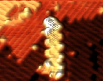
Dry contact transfer is used to press a fiberglass applicator coated with a powder of atomically precise graphene nanoribbons (that had been synthesized in solution and then degassed at high temperature to remove contaminants) against a hydrogen-passivated Si(100) surface under ultrahigh vacuum. The graphene nanoribbons (GNRs) cleanly exfoliate onto the surface. 80 of 115 GNRs imaged using scanning tunneling microscope spectroscopy were nontransparent (the lattice of the underlying Si substrate was not visible) with an average apparent height of 0.30 nm. The GNRs do not appear to align to the Si lattice, indicating a weak coupling interaction. The 35 semitransparent nanoribbons exhibited an average, apparent height of 0.20 nm. Semitransparency is an imaging artifact influenced by tip-sample separation, the work function of the STM probe, nanoribbon-surface interaction, and surface density of states within the GNR energy bandgap.
High resolution scanning tunneling spectroscopy and current imaging tunneling spectroscopy were used to determine the details of the electronic structure of the chevron GNRs and their interactions with the Si surface. Results are compared with previous studies of chevron GNRs on gold and of graphene nanoflakes on H:Si(100). The fact that the graphene lattice is only observed for nontransparent GNRs indicates the carbon plane is at a height near 0.30 nm, and a van der Waals bonding interaction between GNRs and the Si substrate is possible. The interaction between the GNR and the surface is weak enough to allow movement of the GNR using the STM tip. The average bandgap over 21 GNRs was determined to be 2.85 eV with a standard deviation of 0.13 eV.
Dry contact transfer also places overlapping nanoribbons on the surface, allowing the study of multilayer GNRs. Although these multilayer cross-junctions formed accidentally, they could be formed deliberately by manipulation with an STM tip. The effect of GNR junctions on height and band gap were determined. The Si surface under part of a GNR was depassivated by holding the sample bias at 8 V while moving the STM tip over the GNR. The height and width of a GNR are decreased after depassivation, indicating an increased coupling to the Si(100) surface and a change in the electronic structure of the GNR. Metallic behavior after hydrogen depassivation is attributed to changes in the GNR electronic structure caused by Si-C bonding.
First principles DFT simulation were performed before and after hydrogen depassivation. After hydrogen depassivation, the projected density of states of the GNR shows finite states at the Fermi level, and there is no longer a band-gap. The formation of covalent bonds between the Si surface and the GNR leads to metallic behavior. The Si surface atoms move outward, and the GNR changes from flat to distorted, with some C atoms moving in toward the Si surface.
Using their dry contact transfer process, the authors have cleanly placed atomically precise graphene nanoribbons on a technologically relevant semiconductor surface, manipulated GNR position with an STM tip, and demonstrated control over interactions between the nanoribbon and surface using atomically precise hydrogen depassivation. Their conclusion seems well-founded:
The ability to cleanly place atomically precise GNRs onto H:Si(100) is unprecedented and is expected to have an enormous impact on GNR device prototyping.
This work should herald progress toward atomically precise transistors, qubits, and increasingly complex atomically precise nanolithography.
—James Lewis, PhD
Discuss these news stories on Foresight’s Facebook page or on our Facebook group.