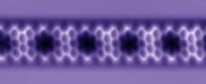
Even without a general method for high throughput atomically precise manufacturing, atomic precision in nanotechnology is proving increasingly useful across a range of technologies. One recent example is the atomically controlled boron-doping of graphene nanoribbons. A hat tip to Science Daily for reprinting this University of Basel news release “Successful Boron-Doping of Graphene Nanoribbon“:
Physicists at the University of Basel succeed in synthesizing boron-doped graphene nanoribbons and characterizing their structural, electronic and chemical properties. The modified material could potentially be used as a sensor for the ecologically damaging nitrogen oxides, scientists report in the latest issue of Nature Communications [“Atomically controlled substitutional boron-doping of graphene nanoribbons” OPEN ACCESS].
Graphene is one of the most promising materials for improving electronic devices. The two-dimensional carbon sheet exhibits high electron mobility and accordingly has excellent conductivity. Other than usual semiconductors, the material lacks the so-called band gap, an energy range in a solid where no electron states can exist. Therefore, it avoids a situation in which the device is electronically switched off. However, in order to fabricate efficient electronic switches from graphene, it is necessary that the material can be switched “on” and “off”.
The solution to this problem lies in trimming the graphene sheet to a ribbon-like shape, named graphene nanoribbon (GNR). Thereby it can be altered to have a band gap whose value is dependent on the width of the shape.
Synthesis on Gold Surface
To tune the band gap in order for the graphene nanoribbons to act like a well-established silicon semiconductor, the ribbons are being doped. To that end, the researchers intentionally introduce impurities into pure material for the purpose of modulating its electrical properties. While nitrogen doping has been realized, boron-doping has remained unexplored. Subsequently, the electronic and chemical properties have stayed unclear thus far.
Prof. Dr. Ernst Meyer and Dr. Shigeki Kawai from the Department of Physics at the University of Basel, assisted by researchers from Japanese and Finnish Universities, have succeeded in synthesizing boron-doped graphene nanoribbons with various widths. They used an on-surface chemical reaction with a newly synthesized precursor molecule on an atomically clean gold surface. The chemical structures were directly resolved by state-of-the-art atomic force microscopy at low temperature.
Towards a Nitrogen Oxide-Sensor
The doped site of the boron atom was unambiguously confirmed and its doping ratio – the number of boron atoms relative to the total number of atoms within the nanoribbon – lay at 4.8 atomic percent. By dosing nitric oxide gas, the chemical property known as the Lewis acidity could also be confirmed.
The doped nitric oxide gas was highly-selectively adsorbed on the boron site. This measurement indicates that the boron-doped graphene nanoribbon can be used for an ultra-high sensitive gas sensor for nitrogen oxides which are currently a hot topic in the industry as being highly damaging to the environment.
The researchers state that the boron-doped graphene nanoribbons they prepare are “well-structured … in terms of valency, position and doping ratio … .” These nanoribbons were built from the bottom up by polymerization of atomically precise components, beginning with the chemical bonding of two pristine anthracene molecules (halogenated at positions 9 and 10) with one 9,10-dibora-9,10-dihydroanthracene moiety. The atomic precision of the results was verified by scanning tunneling microscopy and atomic force microscopy using a molecularly functionalized tip, and by atomistic calculations. The more that pioneering efforts like this establish the advantages of atomically precise materials, the more (we can hope) the need for a convenient, quick, and inexpensive general method of high throughput atomically precise manufacturing becomes apparent.
—James Lewis, PhD
