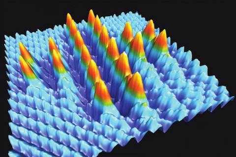

If the above picture reminds you of something like it some 27 years ago when physicists announced a nanostructure built atom-by-atom, then it is important to recognize there are multiple crucial differences between the above 2014 image of a Swiss cross formed from 20 precisely placed bromine atoms and the 1990 image of the IBM logo formed from 35 precisely placed xenon atoms (Foresight Update 9 “Spelling IBM with 35 Atoms” June 30, 1990). The Swiss cross fabrication was reported in a University of Basel press release three summers ago “Smallest Swiss cross in the world made in Basel“:
Researchers at the University of Basel have made the smallest Swiss cross in the world, out of just 20 atoms. It’s the first time a structure of single atoms has been made at room temperature—it normally has to be much colder for the structure to be stable.
The international team in the university’s physics department used the tip of an atomic force microscope, which is extremely tiny and used in nanotechnology, to place the bromine atoms on an insulating surface.
The Swiss cross they constructed measures only 5.6 nanometres square.
Physicists have been able to move around and reposition single atoms since the 1990s, when done at very low temperatures. Attempts to create these types of structures at room temperature however, had produced disappointing results up until now as they were too difficult to control and properly manipulate.
The study, which was published in the journal, Nature Communications [“Atom manipulation on an insulating surface at room temperature“, OPEN ACCESS], states that the researchers have showed that the systematic manipulation of atoms at room temperature is now possible, demonstrating a key step towards a number of new developments, including new atomic-scale data storage devices.
The 1990 paper presenting the IBM logo was done using a scanning tunneling microscope (STM) in ultra high vacuum and very low temperature (4 K) to position individual xenon atoms on a single-crystal nickel surface with atomic precision. The Xenon atoms were adsorbates, not covalently bound to the surface, and so they could be manipulated by the force exerted by the STM tip. That force contains both van der Waals and electrostatic contributions, and adjusting the position and voltage of the tip determines both the magnitude of the force, and whether it is attractive or repulsive.
It generally takes less force to move an atom along the surface than to pull it away from the surface. Therefore, it is usually possible to adjust parameters so that an STM tip can pull an atom across the surface while the atom remains bound to the surface. The decision to study xenon on a Ni (110) surface was dictated by the requirement that corrugations of the surface potential be sufficiently large for the xenon atoms to be imaged without inadvertently moving them, but small enough that enough lateral force could be exerted to move xenon atoms across the surface. Note that although the STM tip is made from tungsten wire, the chemical identity of the tip apex is not known.
The statement in the above University of Basel press release that this demonstration is “the first time a structure of single atoms has been made at room temperature” is not true, although it is true that this was the first instance in which a structure was made on an insulating surface at room temperature. An earlier demonstration was on a semiconductor surface.
The 2009 Foresight Institute Feynman Prize for Experimental work was awarded to the team of Yoshiaki Sugimoto, Masayuki Abe, and Oscar Custance for the use of atomic resolution dynamic force microscopy — also known as non-contact atomic force microscopy (NC-AFM) — for vertical and lateral manipulation of single atoms on semiconductor surfaces at room temperature. This accomplishment was reported in a 2008 paper in Science “Complex Patterning by Vertical Interchange Atom Manipulation Using Atomic Force Microscopy” [abstract] and described in an article in ScienceDaily “Scientists ‘Write’ With Atoms Using An Atomic Force Microscope“.
In this 2008 work NC-AFM using commercial silicon cantilevers with very sharp tips were used to image a Sn/Si (111) reconstructed surface by detecting the short-range chemical interaction force between the closest tip and surface atoms. A vertical interchange of tip and surface atoms was observed controlled by the mechanical properties of a hybrid tip-surface structure formed in the repulsive regime of the tip-surface interaction force.
The surface appears initially as a single atomic layer of tin (Sn) atoms grown over a Si(111) single crystal substrate. The imaged surface exhibited atomic defects consisting of single Si atoms interspersed in the Sn monolayer. After imaging the surface and placing the AFM tip directly over a single Si atom, and moving the surface toward the oscillating AFM tip, at a certain tip-surface distance am instability in the oscillation frequency occurs. Imaging the surface after the tip was retracted showed the Si atom had been replaced by a Sn atom at the same lattice position. Repeating this process multiple times resulted in the atomic symbol for silicon—Si— constructed from 12 Si atoms on a surface of Sn atoms. These manipulations could be accomplished either at room temperature or at the low temperature of 80 K.
The process described above differs from the two other methods of controlled manipulation of isolated atoms by scanning probe microscopes that had been described previous to this publication: (1) using a bias voltage from an STM to drag a weakly bound atom across a metallic surface; (2) using the attractive part of the tip-surface interaction of an AFM to laterally manipulate atoms without any active participation of the AFM tip beyond tuning the interaction of the manipulated atom with the surface.
The bonding interaction between the closest tip and surface atoms in the repulsive regime is complex, involving several atoms and leading to a complex energy landscape that could result in three outcomes: (1) interchange of tip and surface atoms; (2) atom transfer to the tip; (3) deposition of tip atoms on the surface. Simulations based on density functional theory first-principles calculations rationalize the observed result that experiments with many individual tips fall into three classes: (1) some tips alternately deposit Sn and Si atoms; (2) others only deposit Sn atoms; (3) some only deposit Si atoms. The fact that specific classes of tip had to be identified for specific manipulations accounts for the fact that it took 1.5 h to build the ‘Si’ image shown.
The 2014 paper presenting the fabrication of the Swiss cross from 20 bromide ions on an insulator surface notes that since the 1990 atomic manipulation of xenon atoms on a nickel surface, the ultimate goal has been fabrication of next-generation atomic-scale electro-mechanical devices operating at room temperature (RT) on a dielectric surface (an electrical insulator that can be polarized by an electric field). The paper further notes that on fully insulating surfaces, the smaller diffusion barrier of adsorbed species compared to covalently bounded semiconductor surfaces makes room temperature mechanical manipulation by AFM more difficult than on semiconductor surfaces. This paper presents “the first systematic atomic manipulation on an insulating NaCl(001) surface under ultra-high vacuum (UHV) conditions at RT.”
These experiments use “the recently developed bimodal dynamic mode AFM (bimodal d-AFM, a 2009 paper with the same first and last authors as this 2014 paper), in which the vertical and lateral tip-sample interactions are simultaneously detected via frequency shifts of the flexural and torsional resonance modes, respectively.” These changes result in improved resolution at the atomic scale. The tip apex of a silicon cantilever was terminated with NaCl by prior indentation to the sample surface. Imaging a 28 nm x 28 nm area with the bimodal technique revealed the typical contrast pattern of a NaCl (100) surface, with a number of defects appearing as brighter atomic sites. These were attributed to contaminating bromide ions, whose presence in the crystal was confirmed by X-ray fluorescence analysis. The concentration of bromide ions estimated by AFM was one order of magnitude higher than the crystal concentration. This difference was attributed to the effect of annealing the NaCl crystal at 80 °C. FroM their AFM images, the authors conclude that the foremost atom on the tip apex must be a sodium ion (Na+) and that the corrugation amplitude of bromide ion is about three times higher than the corrugation amplitude of chloride ion, and that the position of the bromide ion is predicted to be 20 pm (picometers) above the surface. They further conclude that the bromide ions are not adsorbed on the surface, but instead incorporated into the NaCl(001) surface layer as substitutional species in the Cl– sub-lattice. Further, the bromide ions were stable to repeated imaging over the time course of the experiment.
Upon scanning at smaller tip-sample separations, a class of novel lateral manipulations appears in which a bromide ion exchanges with a chloride ion while scanning in a specific direction. The diversity of this class of lateral manipulations indicated to the authors that the mechanism is more complicated than is the case with a standard lateral manipulation in which an adatom moves on top of the surface.
To achieve more control in manipulating bromide ions, an equivalent of dynamic force spectroscopy was attempted by sequentially approaching the surface to pick up the ion, and then approaching the surface again to implant the ion at the desired surface lattice location. 95 % of the implantations were successful. The experimental data reveal that implantation only occurs if the tip is approached 100 pm closer than the pickup approach.
Theoretical calculations of the manipulation mechanisms based on density functional theory (DFT) were performed In order to understand the detailed process of the atomic manipulation. The model system included a NaCl nanocluster tip and the NaCl surface with one substitutional bromide ion. Conventional lateral manipulation has too high a transition barrier to account for the extensive lateral manipulation observed experimentally. The authors suggest a more plausible model involving the tip temporarily picking up a bromide ion, allowing the vacancy underneath to diffuse before the bromide ion is dropped into a new site. They note that the barrier for vacancy diffusion is always low, and proximity to the tip reduces the barrier to lifting the bromide ion above the surface, especially if a polar model of the tip is used. Thus this process is only viable at large tip-sample separations and is not directionally controlled.
In contrast to the more random lateral manipulationprocess, the statistical preference for implanting ions over picking up ions at closer approach made i possible to perfectly align 20 broide ion in the NaCl surface, forming a 5.64 nm by 5.64 nm ‘Swiss cross’. The authors note that this was the largest number of atomic manipulations achieved at room temperature. They further note that bromide ions are positioned at every other chloride ion site on the surface, and that the fabricated cross is “relatively stable” in that no diffusion was observed during the six hours it took to build the structure. Thus, combining theory with the bimodal dynamic force microscopy they had published five years earlier, they were able to demonstrate “how systematic atomic manipulation at RT, on any class of surface, is now possible. This is an important step towards the fabrication of advanced electromechanical systems at the nanoscale, in a bottom-up manner.” This 2014 advance has capped a 24-year journey to build a larger variety of structures on a surface, atom-by-atom, but I expect that this will not be the end of the story, and that scanning probe microscopes will continue to figure prominently in the roadmap to productive nanosystems and atomically precise manufacturing.
—James Lewis, PhD
Discuss these news stories on Foresight’s Facebook page or on our Facebook group.