
Soon after graphene sheets were being produced on a laboratory scale routinely, researchers began producing the hydrogenated version graphane (with a hydrogen atom on each carbon). This step is one of many approaches aimed at harnessing graphene’s powerful conductivity and is also being explored for hydrogen storage and other potential applications (more info in this 2009 ScienceDaily article From Graphene to Graphane…). Despite the divergence from planarity which naturally accompanies the shift from sp2 to sp3 hybridization, graphane is considered a 2D material.
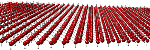
Brought to our attention by Christine Peterson, a new addition to the family of 2D honeycomb-lattice materials has arrived: germanane. Structurally analogous to graphane, germanane comprises hydrogenated, hexagonally arranged germanium atoms in single (or few) layer sheets. Like silicane and silicene (see companion post Silicene: silicon’s answer to graphene), germanane should have a band gap, possibly allowing it to be implemented sooner than graphene.
While bulk germanium was semi-successfully used to make the first transistors, its low resistivity at higher temperatures and high production costs limited its practical use, and silicon soon became the semiconductor of choice. But going nanoscale may be a game changer, if the right combination of performance, cost, and ease of manufacture can be found.
For most 2D materials, getting stable sheets is the first hurdle. In an important step toward production of germanane sheets, a research team led by Joshua Goldberger at Ohio State University has devised a method for chemical synthesis of germanane crystals, which can be exfoliated down to single layer sheets. The work is published in ACS Nano (abstract) and is described in a Gizmag article:
“…we’ve been searching for unique forms of silicon and germanium with advantageous properties, to get the benefits of a new material but with less cost and using existing technology.”
The resulting material has been shown to conduct electrons ten times faster than silicon (and five times faster than conventional germanium), meaning that it could carry a proportionately higher load if used in microchips. It’s also more chemically stable than silicon, not oxidizing in the presence of air or water, plus it’s much better at absorbing and emitting light – this means that it could prove particularly useful in solar cells.
Ordinarily, germanium takes the form of multilayered crystals. The single-atom-thick layers are bonded to one another, and each one is quite unstable on its own. The OSU researchers created their own germanium crystals, in which calcium atoms were inserted between the layers. That calcium was then dissolved using water, leaving empty chemical bonds in its absence. Those bonds were subsequently plugged with hydrogen, resulting in much more stable layers that could be peeled from the crystal while remaining intact.
A down side of germanium-based technologies may still be cost – germanium is far less abundant than silicon and carbon. From a Productive Nanosystems point of view, graphene technology may prevail in the long run due not only to performance metrics but to the abundance of carbon as well. For nearer-term, intermediate technologies, many hats remain in the ring. Although Group 14 elements are highlighted here, serious research into a broad range of 2D (especially honeycomb structured) materials has been around for a while and is growing fast.
-Posted by Stephanie C