
A decade ago Foresight participated in a two-year effort to produce the first technology roadmap from current, incremental nanotechnology to productive nanosystems capable of general purpose, high-throughput atomically precise manufacturing (APM). The purpose of roadmaps, such as the well-known and extremely successful International Technology Roadmap for Semiconductors, is to define the future technology requirements for complex systems so that present-day research world-wide can be coordinated to develop all the necessary components for the future target system, be it a next generation semiconductor fabrication facility for computer chips, or a nanofactory.
With ITRS the challenge is to develop the next generation of a mature, commercially successful technology. With APM the first generation does not yet exist so the challenge is how to go from a set of disparate enabling technologies, including various molecular sciences and surface physics, to the first functional prototype of a nanofactory. With ITRS the current and earlier technology generations have enabled a flourishing industry that lies at the foundation of much of the world economy and has vast financial resources, providing ample incentive to develop the next generation of the technology. With APM there is no legacy of previous generations, so the incentive to develop the first generation has to come from industries and needs served by different technologies (molecular sciences like chemistry and biotechnology, materials science) that could benefit by extension or replacement of those technologies with APM.
In a blog post several years ago, Eric Drexler tackled the question of how to provide roadmaps in an area of technology for which the practical physical implementation of the technology remains uncertain, and pointed to the Quantum Information Science and Technology Roadmap as an example. Perhaps another way to approach this question is to ask what can be learned from a roadmap in (current-day, incremental) nanotechnology, as defined by the US National Nanotechnology Initiative as “… the understanding and control of matter at the nanoscale, at dimensions between approximately 1 and 100 nanometers, where unique phenomena enable novel applications.” Does such a roadmap exist? Foresight Co-Founder Christine Peterson forwarded this story from Nanowerk News of one such roadmap resulting from a call by the European Commission “The European nanotechnology roadmap for graphene“:
In October 2013, academia and industry came together to form the Graphene Flagship. Now with 142 partners in 23 countries, and a growing number of associate members, the Graphene Flagship was established following a call from the European Commission to address big science and technology challenges of the day through long-term, multidisciplinary R&D efforts.
In a 200-page open-access paper published in the Royal Society of Chemistry journal Nanoscale (“Science and technology roadmap for graphene, related two-dimensional crystals, and hybrid systems“), more than 60 academics and industrialists lay out a science and technology roadmap for graphene, related two-dimensional crystals, other 2D materials, and hybrid systems based on a combination of different 2D crystals and other nanomaterials. The roadmap covers the next ten years and beyond, and its objective is to guide the research community and industry toward the development of products based on graphene and related materials. …
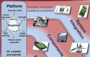
The roadmap highlights three broad areas of activity. The first task is to identify new layered materials, assess their potential, and develop reliable, reproducible and safe means of producing them on an industrial scale. Identification of new device concepts enabled by 2D materials is also called for, along with the development of component technologies. The ultimate goal is to integrate components and structures based on 2D materials into systems capable of providing new functionalities and application areas.
Eleven science and technology themes are identified in the roadmap. These are: fundamental science, health and environment, production, electronic devices, spintronics, photonics and optoelectronics, sensors, flexible electronics, energy conversion and storage, composite materials, and biomedical devices. The roadmap addresses each of these areas in turn, with timelines. …
Having only devoted a few minutes to a very cursory look at this very substantial report, I can only make a few initial observations at this point:
- A very impressive survey is presented of nearly a dozen technical areas, including looking in some depth at the opportunities and requirements in each area.
- These surveys seem to indicate the need for ever greater control of the structure of matter at the nanoscale, in many cases extending toward atomic precision to achieve the ultimate possible function.
- A common theme in many areas seems to point to reliable and inexpensive fabrication as a major problem to be solved.
I was struck by these points from the Conclusions of the report:
… the availability of a product for the end user is strictly dependent on the different pace of the material development. The cheapest GRMs and with the least stringent requirements could be the first available on the market …
The target is to develop novel applications, planned thanks to each GRM unique properties, rather than try to replace other materials in existing applications. GRMs will replace existing standard materials only if the properties of the new components are amply competitive to justify the cost for changing current industrial processes.
Given the above, it seems that this report, at the very least, helps to document the opportunities and needs for a general purpose APM. Beyond that, closer study might reveal possible areas of synergism between furthering the development and commercialization of these existing nanotechnologies and steps to develop more capable APM technologies.
—James Lewis, PhD