
Bulk piezoelectric materials are already used for atomically precise nanopositioning to position the tips of scanning probe microscopes. Would there be any advantages to engineered control of piezoelectrical properties in a two-dimensional material? Currently piezoelectric properties of materials cannot be engineered—it is a property only available in certain 3D crystals. Now calculations have demonstrated that graphene can be made piezoelectric by adsorbing atoms on one surface. A hat tip to Physorg.com for reprinting this Stanford University news release written by Andrew Myers “Straintronics: Engineers create piezoelectric graphene“:
Graphene is a wonder material. It is a one-hundred-times-better conductor of electricity than silicon. It is stronger than diamond. And, at just one atom thick, it is so thin as to be essentially a two-dimensional material. Such promising physics have made graphene the most studied substance of the last decade, particularly in nanotechnology. In 2010, the researchers who first isolated it shared the Nobel Prize.
Yet, while graphene is many things, it is not piezoelectric. Piezoelectricity is the property of some materials to produce electric charge when bent, squeezed or twisted. Perhaps more importantly, piezoelectricity is reversible. When an electric field is applied, piezoelectric materials change shape, yielding a remarkable level of engineering control.
Piezoelectrics have found application in countless devices from watches, radios and ultrasound to the push-button starters on propane grills, but these uses all require relatively large, three-dimensional quantities of piezoelectric materials.
Now, in a paper published in the journal ACS Nano [abstract], two materials engineers at Stanford have described how they have engineered piezoelectrics into graphene, extending for the first time such fine physical control to the nanoscale.
“The physical deformations we can create are directly proportional to the electrical field applied. This represents a fundamentally new way to control electronics at the nanoscale,” said Evan Reed, head of the Materials Computation and Theory Group at Stanford and senior author of the study.
This phenomenon brings new dimension to the concept of ‘straintronics,’ he said, because of the way the electrical field strains—or deforms—the lattice of carbon, causing it to change shape in predictable ways.
“Piezoelectric graphene could provide an unparalleled degree of electrical, optical or mechanical control for applications ranging from touchscreens to nanoscale transistors,” said Mitchell Ong, a post-doctoral scholar in Reed’s lab and first author of the paper.
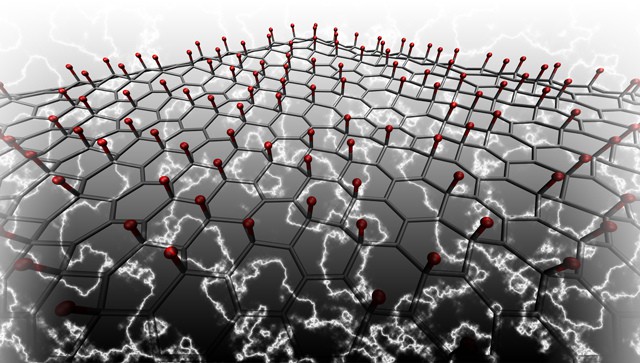
Using a sophisticated modeling application running on high-performance supercomputers, the engineers simulated the deposition of atoms on one side of a graphene lattice — a process known as doping — and measured the piezoelectric effect.
They modeled graphene doped with lithium, hydrogen, potassium and fluorine, as well as combinations of hydrogen and fluorine and lithium and fluorine on either side of the lattice. Doping just one side of the graphene, or doping both sides with different atoms, is key to the process as it breaks graphene’s perfect physical symmetry, which otherwise cancels the piezoelectric effect.
The results surprised both engineers.
“We thought the piezoelectric effect would be present, but relatively small. Yet, we were able to achieve piezoelectric levels comparable to traditional three-dimensional materials,” said Reed. “It was pretty significant.”
The researchers were further able to fine tune the effect by pattern doping the graphene—selectively placing atoms in specific sections and not others.
“We call it designer piezoelectricity because it allows us to strategically control where, when and how much the graphene is deformed by an applied electrical field with promising implications for engineering,” said Ong.
While the results in creating piezoelectric graphene are encouraging, the researchers believe that their technique might further be used to engineer piezoelectricity in nanotubes and other nanomaterials with applications ranging from electronics, photonics, and energy harvesting to chemical sensing and high-frequency acoustics.
“We’re already looking at new piezoelectric devices based on other 2D and low-dimensional materials, hoping they might open new and dramatic possibilities in nanotechnology,” said Reed.
Could piezoelectric graphene be used with, for example, DNA origami scaffolding to position molecular tools to execute programmed actions? To hear the researchers discussing their work and plans, including possible application to nanomechanical systems, an ACS Nano podcast is available.
—James Lewis, PhD