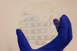
By precise control of several factors, uniform high-performance monolayers of the semiconductor MoS2 have been obtained and used to fabricate field-effect transistors.
By precise control of several factors, uniform high-performance monolayers of the semiconductor MoS2 have been obtained and used to fabricate field-effect transistors.
Even without special designs and coatings to promote stability, simple DNA nanomachines can survive in human serum and blood for hours or even days, much longer than expected from previous studies using bovine serum, which has more damaging nucleases than does human serum.
Designing and building spiroligomers, robust building blocks of various 3D shapes made from unnatural amino acids, decorated with various functional groups, and linked rigidly together by pairs of bonds, and a new approach to nanotechnology design software.
A US government Request for Information (RFI) is seeking suggestions for Nanotechnology-Inspired Grand Challenges for the Next Decade. The manufacture of atomically-precise materials is offered as #4 of 6 examples.
At the 2013 Conference George Church presented an overview of his work in developing applications of atomically precise nanotechnology intended for commercialization, from data storage to medical nanorobots to genomic sequencing to genomic engineering to mapping individual neuronal functioning in whole brains.
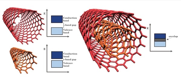
Density functional theory calculations of the electronic properties of double-walled carbon nanotubes (DWCNTs) comprising two concentric zigzag tubes of different chiralities reveal complex effects upon the electronic band gap, identifying candidate combinations for diverse applications from transistors to macroscopic conducting wires.
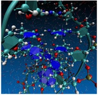
A combination of techniques has made possible the expansion of problems that can be handled by first-principles molecular dynamics from a few hundred atoms to a very large system containing 32,768 atoms.
A very efficient and scalable method of completely removing metallic carbon nanotubes from mixtures of metallic and semiconducting carbon nanotubes produces arrays suitable for many applications and for studies of thin film transistors.
Programmed assembly and disassembly of rigid 3D DNA origami objects has been achieved by designing complementary surface shapes based upon weak stacking interactions to create simple nanomachines.
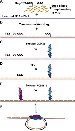
Linking proteins to DNA scaffolds to produce complex functional nanostructures can require chemistry that damages protein function. A new systematic approach avoids exposing proteins to damaging conditions.